Electrokinetic micro power cell using microfluidic-chip with multi-channel type

Inactive Publication Date: 2006-04-20
KOREA INST OF SCI & TECH
6 Cites 13 Cited by

AI-Extracted Technical Summary

Problems solved by technology

However, above research is limited to the 1:1 type electrolyte solution with low surface potential because the Debye-Hückel approximation is...

Benefits of technology

[0027] An electrokinetic micro power cell according to the present invention can efficiently get el...

Abstract

The invention relates to a new micro power cell applying the microfluidic-chip with multi-channel type. The streaming potential is the main thrust, which is created by Helmholtz-Smoluchowski's electrokinetic principle when electrolytic solution flows through a microchannel. The microfluidic-chip comprises an inflow port, a distributor, a multi-channel, a collector, an outflow port, and a pair of electrodes. The present invention could be applied to a new power source of clean energy.

Application Domain

Immobilised enzymesBioreactor/fermenter combinations +13

Technology Topic

Microfluidic chipElectrical battery +7

Image

  • Electrokinetic micro power cell using microfluidic-chip with multi-channel type
  • Electrokinetic micro power cell using microfluidic-chip with multi-channel type
  • Electrokinetic micro power cell using microfluidic-chip with multi-channel type

Examples

  • Experimental program(3)

Example

Embodiment 1 Fabrication of Master Mold for Making a Microfluidic-Chip Device with a Multi-Channel Type According to the Invention
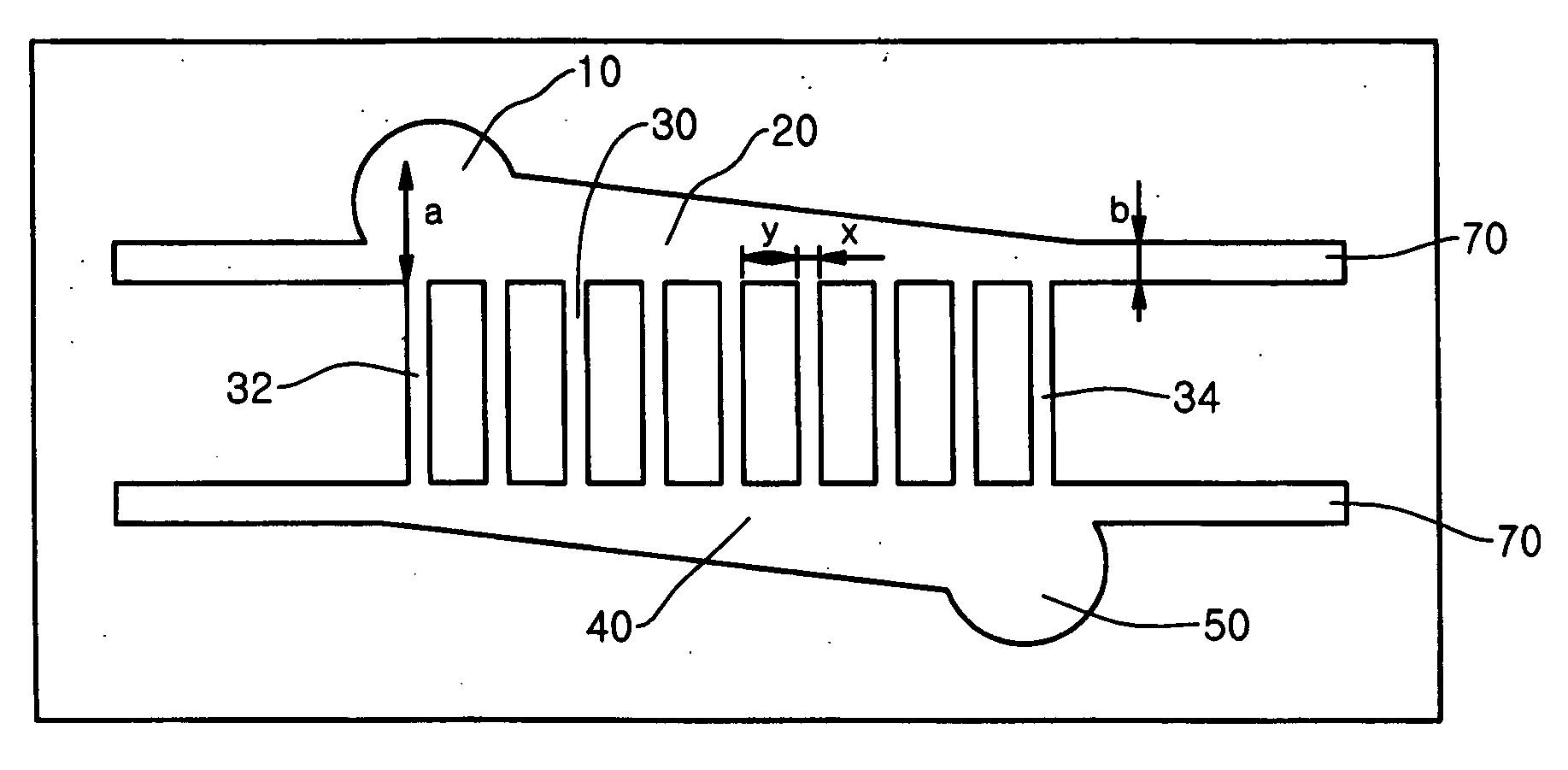
[0067]FIG. 1 depicts a photomask drawing designed by AutoCAD® 2002 as a first step for making the microfluidic-chip according to the invention. The chip includes the inflow port 10, the distributor 20, the multi-channel 30, the collector 40, and the outflow port 50.
[0068] In the distributor 20 and the collector 40, Ag/AgCl electrodes should be inserted. Therefore, the distributor 20 and the collector 40 should be formed in the depth enough to place the electrodes in them. Similarly, the multi-channel 30 consisting of 100 microchannels should be formed to the same depth as the distributor 20 and the collector 40. Because the diameter of conventional electrodes has about 100 μm, it is optimum to form the microchannel depth to be about 100 μm.
[0069] The diameter of the inflow port 10 into which fluid flows and the outflow port 50 from which fluid flows out may be determined to properly connect the inflow port 10 and the outflow port 50 to external tubes. In the embodiment, external tubes have 1/16 inch diameter, the diameter of the inflow port 10 and the outflow port 50 is set in 1.6 mm.
[0070] In order to place the electrodes at the input side as well as the output side of the multi-channel, the electrode insertion space 70 is formed. The width of the electrode insertion space is designed to be suitable to insert the electrode therein, which is set to be 300 μm in this embodiment. As the inserted electrode in this embodiment is an Ag wire in 100 μm diameter and its surface is coated with AgCl, 200% space margin to the diameter of the Ag wire is reserved.
[0071] The distributor 20 having the fluid supplied through the inflow port 10 flow uniformly into the multi-channel, and the 40 collecting the fluid flowed out from the multi-channel preferably take a trapezoidal shape. The cross-sectional area of the distributor 20 decreases from the one side 32 located the inflow port to the opposite side 34. Also, the cross-sectional area of the collector 40 decreases from the one side 34 located the outflow port to the opposite side 32.
[0072] In case of being designed as such, when the fluid flows through 100 of the microchannels, the fluid can almost simultaneously flow out from the outlet of the multi-channel as described above. If the distributor is designed in a uniform width as the rectangular shape, the fluid flowing into the microchannel 32 located at the side where the inflow port 20 exists flows possibly out to the collector 40 before the fluid flows into the microchannel 34 located at the opposite side. In this case, the electrical energy will not regularly generate since the electric potential difference decreases extremely.
[0073] In the distributor 20 and the collector 40 taking a trapezoidal shape, the decreasing rate of the width r is estimated depending on the total length L determined by the channel width x, the spacing between microchannels y, and the number of microchannels N. When the length of longer-side and that of shorter-side in the trapezoid denote a and b respectively, the decreasing rate of the width r is defined by equation 2. r ≡ a - b L = a - b N ⁢ ⁢ x + ( N - 1 ) ⁢ y [ Equation ⁢ ⁢ 2 ]
[0074] In the mask design according to this embodiment, parameters are as follows: the length of longer-side a is 800 μm, the length of shorter-side b is 300 μm, the channel width x is 20 μm, the spacing between microchannels is 100 μm, and the number of channels is 100. In this case, the decreasing rate r of the width is 0.042.
[0075]FIG. 2 depicts a process flowchart for fabricating the microfluidic-chip with multi-channel type. FIG. 3a through FIG. 3e depict cross-sectional views for fabricating the microfluidic-chip.
[0076] At first, the mask is designed as explained above (S10, FIG. 1).
[0077] The surface of silicon wafer is washed with piranha solution made by mixing H2SO4 and H2O2 in the ratio of 1:4. Then, a photoresist SU8-50 (MicroChem Co., MA) 200 is layered on the silicon wafer 100 by spin coating (S20, FIG. 3a). As described above, in order that the microchannel depth is to be 100 μm, the photoresist is accumulated 100 μm in thickness. The coating thickness varies depending on the revolution rate of spin coating. SU8-50 spreads out uniformly on the wafer with revolution 500 rpm for 10 seconds, and then, with acceleration 300 rpm/sec and revolution 1000 rpm for 30 seconds to take the thickness of 100 μm.
[0078] Then, the coated wafer is soft-baked on a hot plate for 10 minutes at 65° C., and for 30 minutes at 95° C. (S30). As the photoresist SU8-50 is sensitive to heat, therefore, temperature is raised slowly from the room temperature to 65° C. and 95° C. without abrupt heating.
[0079] The soft-baked wafer is patterned by exposing to i-line (365 nm wavelength of UV range) with MA6 mask aligner (S40). When it is exposed for 60 seconds in the energy density of 17 mW/m2 through the photomask fabricated in the step of S10, the photoresist exposed to lights is cross-linked.
[0080] The exposed SU8-50 is fixed more tightly on the wafer 100 through the post exposure baking (S50).
[0081] Then, through the developing procedure by agitating with a magnetic bar, a portion of SU8-50 200 not exposed to the lights is eliminated by melting in the developer to form the master mold (S60, FIG. 3b). Soaking for too much time provides undesirable separations of any portion of SU8-50 200 exposed to the lights from the wafer. Therefore, attention is needed in this step.
[0082]FIG. 6 depicts a picture of the fabricated master mold. The photoresist SU8-50 is patterned in 100 μm thickness on a silicon wafer with 4 inch diameter. The master mold has been designed variously in dimension and geometry of the microchannel.
[0083] In the picture of FIG. 6, the right-half side and the left-half side demonstrate each mold with 100 μm and 50 μm of spacing between microchannels, respectively.
[0084] In addition, the upper-half side and the lower-half side demonstrate each mold with 1 mm and 3 mm of microchannel length, respectively. As getting away from the center, the channel width increases to 20 μm, 30 μm, 40 μm, and 50 μm. Both the leftmost and the rightmost in the picture are molds with 100 μm channel width.
[0085]FIG. 7 is a micrograph of microchannels with 20 μm width, 1 mm length, and 100 μm spacing between microchannels, which is taken by microscope with magnifying 20 times of the master mold depicted in FIG. 6.
[0086] Preliminary tubes 15, 55 with 1/16 inch diameter are weakly adhered to and stand at the corresponding positions of the inflow port 10 and the outflow port 50 in the master mold, respectively (S70, FIG. 3c).
[0087] PDMS (Sylgard 184 elastomer, Dow Corning Corp., MI) prepolymer is mixed with a curing agent in a ratio of 10:1 by weight, and then the mixture is poured over the master mold. It is degassed in a vacuum oven, where the oven is made vacuum through 3 or 4 steps for 15˜20 minutes per each step. When all the air bubbles are eliminated, the master mold with PDMS is heated for 2 hours at 80° C. in a convection oven at the atmospheric pressure, and then, it is cooled slowly at room temperature for about 6 hours to cure PDMS 300 (S80, FIG. 3d).
[0088] Then, the preliminary tubes are eliminated, and the cured PDMS 300 is peeled from the master mold. The PDMS 300 is washed by ultra-sonication together with the glass coverslip 400 using methanol for 1 hour.
[0089] Then, the surface of the PDMS and the glass coverslip that are to be sealed each other is treated with O2 plasma by RF power for 10 seconds. The O2 plasma is set in advance to have 50% of partial pressure using RIE apparatus.
[0090] The surface-activated PDMS 300 is adhered to the glass coverslip 400 as quickly as possible to form the microfluidic-chip (S90, FIG. 3e). The microfluidic-chip can withstand up to about 5 bar between both ends of the microchannel.
[0091] Then, the electrodes 60 are inserted in the electrode insertion space 70 at both ends of microchannels of the chip (S100). After eliminating the preliminary tubes, permanent tubes 150, 151 (FIG. 4a) are inserted and fixed by an epoxy resin and an adhesive for silicon rubber (S110).
[0092]FIG. 4a is a perspective view of the microfluidic-chip fabricated by the above method. FIG. 4b and FIG. 4c depict cross-sectional view taken along with A-A′ line and B-B′ line in FIG. 4a, respectively.

Example

Embodiment 2 Fabrication of a Streaming Potential Cell
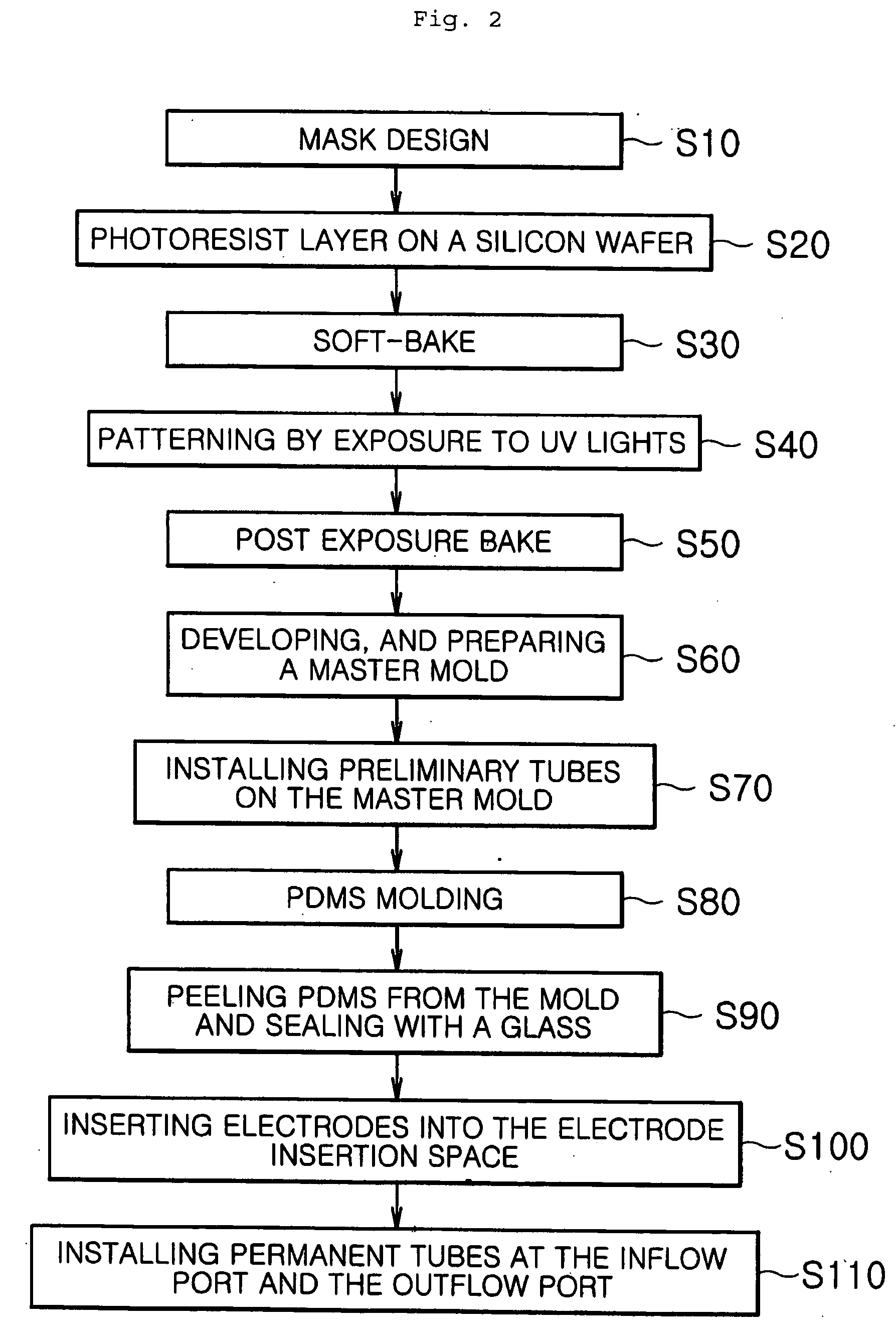
[0093] Before inserting electrodes, an Ag wire (Aldrich Chemical Co., WI) with 100 μm diameter to use as the electrode is washed in 3M HNO3 solution for 5 minutes. Then, the anode (red color) of a power supply is connected to the Ag wire and the cathode (black color) is connected to a Pt wire in 0.1M HCl solution, and then, 4 mA/cm2 of static current is applied for 20 minutes to anodize. AgCl coats the surface of Ag wire, and then an Ag/AgCl electrode can be prepared.
[0094] The Ag/AgCl electrodes are inserted into the electrode insertion space 70 of the microfluidic-chip of the invention.
[0095] Cutting both ends of the PDMS replica peeled from the master mold gives to form holes at both ends of the electrode insertion space in 300 μm width and 100 μm depth. After that, an electrode is inserted into the hole, and the electrode is protruded outside from both ends of the electrode insertion space. Then, the Ag/AgCl electrode is connected to an external Ag wire in 250 μm diameter by Ag soldering on the PCB. The external Ag wire connects to a digital multi-meter through a connector.
[0096] The permanent tubes 150, 151 are installed at the inflow port 10 and the outflow port 50. The electrical energy generated from the chip is available by installing the microfluidic-chip on the PCB.
[0097] In a single channel chip, the range of the endurable pressure is relatively high since the PDMS portion sealed with a glass coverslip is large. In the chip with multi-channel, however, spacing between channels should be adjusted to obtain the appropriate endurable pressure.
[0098] In the above embodiment, the spacing between microchannels is designed at 100 μm, in which patterning in the UV exposure process could be performed without any problem. However, if the spacing is too small (for example, below 50 μm), the patterning may be performed incompletely.
[0099] The portion of the PDMS produced by 100 μm of spacing between channels is activated by the O2 plasma and is to be adhered to the glass coverslip. In order to withstand about 5 bar, this portion of PDMS between channels arranged in parallel each other should be tightly bonded with a glass coverslip. If a channel depth is 100 μm, the spacing between channels may preferably be larger than 100 μm. Therefore, the aspect ratio of the spacing between channels and the channel depth should preferably be designed in 1:1.
[0100]FIG. 8 depicts a streaming potential cell wherein a microfluidic-chip is installed on a PCB. In the microfluidic-chip, external tubes made of polyethylethylketone (PEEK) are inserted by using an epoxy resin and an adhesive, and Ag/AgCl electrodes are inserted and fixed by using an epoxy resin.

Example

Embodiment 3 Measurement Experiments for Electric Potential with a Micro Power Cell According to the Invention
[0101] As shown in FIG. 5, a streaming potential cell is comprised in an electrokinetic micro power cell. In FIG. 5, the fluid that is electrolyte solution contained in a reservoir is supplied into the inflow port 10 by a high-precision metering pump (SD-200, Rainin, Calif.), and it is drained to the outflow port 50 after flowing through the multi-channel 30. The pressure difference ΔP between both ends of microchannels 30 is measured by a precise pressure gauge. The streaming potential difference ΔE between both ends of channels is measured by a digital multi-meter (HP34970A, Hewlett-Packard Co., CA) via the Ag/AgCl electrodes 60 placed respectively at upper and lower parts of the channels. By having electrolyte solution with various ionic concentrations flow, the streaming potential is measured.
[0102]FIG. 9 depicts results of the streaming potential generated depending on the channel width for the deionized water with 10−4 mM ionic concentration, 0.1 mM and 1.0 mM KCl electrolyte solutions. In the micro power cell according to the invention, the number of microchannels is 100, the spacing between channels is uniformly 100 μm, and the flow rate of the solution is set 10 ml/min.
[0103] In the above FIG. 9, in case of the deionized water, the streaming potential is generated up to 700 mV at 20 μm channel width.
[0104]FIG. 10 depicts results of streaming potential coefficients measured by average pressure exerted on both ends of microchannel depending on the channel width for the deionized water, 0.1 mM and 1.0 mM KCl electrolyte solutions. As the channel width increases, the thickness of the electric double layer decreases relatively even in the same ionic concentration. Thus, the value of streaming potential decreases.
[0105]FIG. 11 displays the results of streaming potential depending on the ionic concentration of the electrolyte solution. As depicted in the FIG. 11, as the ionic concentration increases, the thickness of the electric double layer decreases. Therefore, even though channel width is same, the value of streaming potential decreases with increasing the ionic concentration.
[0106] The invention relates to an electrokinetic micro power cell applying the microfluidic-chip with multi-channel type, and could be used as a new power source of clean energy.
[0107] Especially, since it acts as a power supply or self-power chip, it could be used in electrophoresis, optical experimental facilities, ultra small-scale devices for MEMS process such as micro pump, and for charging small electronic devices such as laptop computer or cell-phone.

PUM

PropertyMeasurementUnit
Length2.0E-5 ~ 1.0E-4m
Length0.001 ~ 0.003m
Length5.0E-5 ~ 2.0E-4m

Description & Claims & Application Information

We can also present the details of the Description, Claims and Application information to help users get a comprehensive understanding of the technical details of the patent, such as background art, summary of invention, brief description of drawings, description of embodiments, and other original content. On the other hand, users can also determine the specific scope of protection of the technology through the list of claims; as well as understand the changes in the life cycle of the technology with the presentation of the patent timeline. Login to view more.
Why Eureka
Try Eureka