

Semiconductor memory element and semiconductor memory device
a memory element and semiconductor technology, applied in the direction of information storage, static storage, digital storage, etc., can solve the problems of large circuits peripheral to memory cells, memory cells cannot be made smaller or driven at a lower voltage, and the thin film surrounding the floating gate cannot be as thin as desired
- Summary
- Abstract
- Description
- Claims
- Application Information
AI Technical Summary
Benefits of technology
Problems solved by technology
Method used
Image

Examples
first embodiment
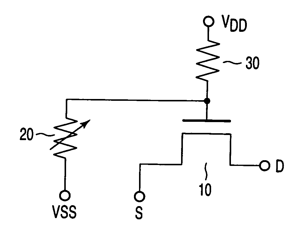
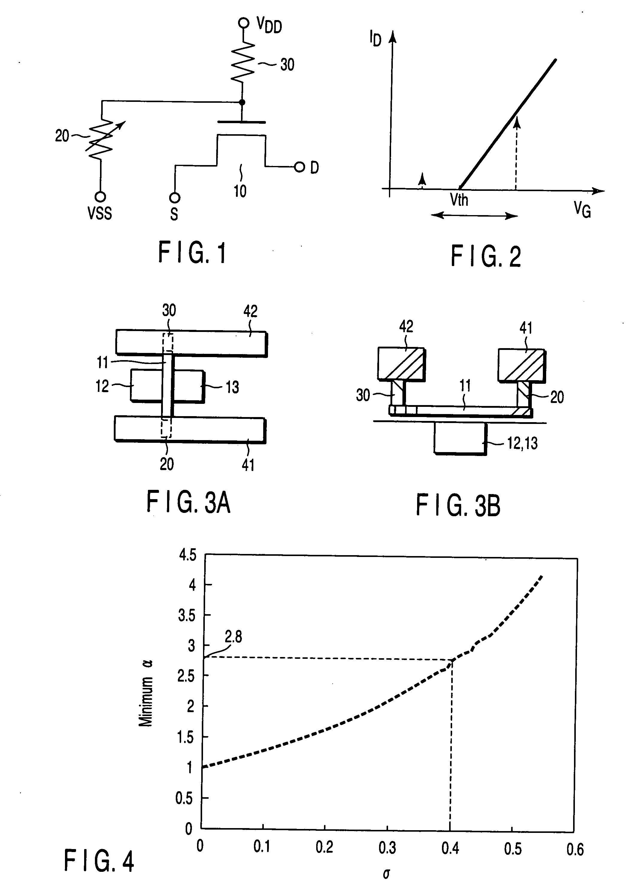
[0030]FIG. 1 is a circuit diagram showing a semiconductor memory element according to the first embodiment of the invention. The memory element shown here is one of the components (i.e., memory cells) that constitute a memory array.
[0031] As FIG. 1 shows, the memory element comprises a metal oxide semiconductor (MOS) transistor 10, a variable resistor element 20, and a resistor 30 (fixed resistor element). The variable resistor element 20 is connected at one end to the gate of the MOS transistor 10 and at the other end to the first power-supply terminal (e.g., ground terminal VSS terminal). The resistor 30 is connected at one end to the gate of the MOS transistor 10 and at the other end to the second power-supply terminal (e.g., power-supply terminal VDD). The variable resistor element 20 is made of, for example, phase-changing material. Its resistance varies with the temperature to which it is heated. More precisely, the variable resistor element 20 has either first resistance or ...
second embodiment
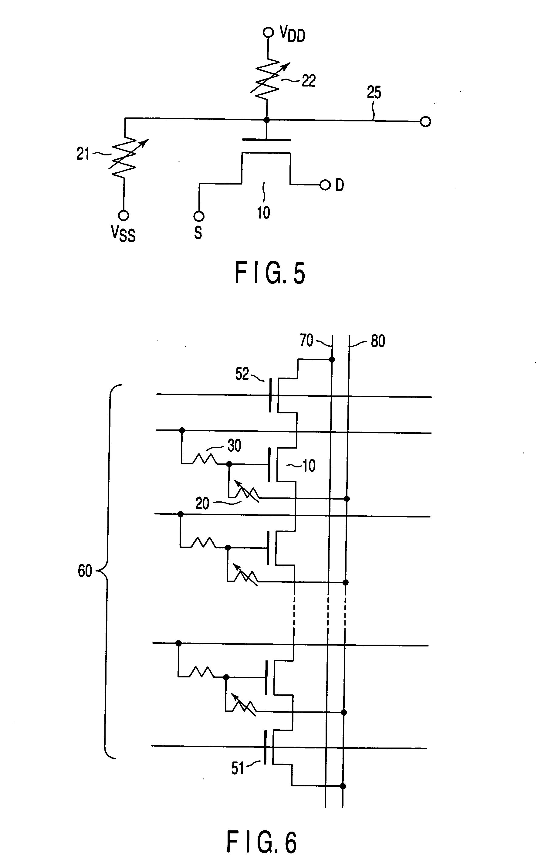
[0065]FIG. 5 is a circuit diagram that illustrates a semiconductor memory element according to the second embodiment of the present invention. More precisely, FIG. 5 depicts the structure of the smallest units (i.e., memory cells) that constitute a memory array.
[0066] The second embodiment differs from the first embodiment in that a control node 25 is provided as an additional component. As FIG. 5 show, a first variable resistor element 21 is connected between the gate of a MOS transistor 10 and the first power-supply terminal (e.g., ground terminal VSS). And a second variable resistor element 22 is connected between the gate of the MOS transistor 10 and the second power-supply terminal (e.g., power-supply terminal VDD). The control node 25 is led from the gate of the MOS transistor 10.
[0067] In the first embodiment, the variable resistor element 20 and the resistor 30 are connected in series. In the second embodiment, the element 22 functions as a variable resistor element becaus...
third embodiment
[0071]FIG. 6 is a circuit diagram showing a semiconductor memory device that is the third embodiment of the present invention.
[0072] More specifically, FIG. 6 depicts one of the blocks constituting a memory cell array, which includes memory cells of the type shown in FIG. 1. Memory cells of the type shown in FIG. 1 are connected in series, providing a series circuit. Two selection transistors are connected to the ends of this series circuit. The block shown in FIG. 6 and other identical blocks are arranged in rows and columns and are connected to one another, constituting the memory cell array.
[0073] As shown in FIG. 6, transistors 10 identical to the transistor included in the memory cell of FIG. 1 are connected in series, constituting a memory cell unit. The first selection transistor 51 is connected between the ground node of the memory cell unit and a source line 80. The second selection transistor 52 is connected between the power-supply node of the memory cell unit and a bit...
PUM
 Abstract
Description
Claims
Application Information