Method for producing a liquid crystal panel

a liquid crystal panel and production method technology, applied in the field of liquid crystal panel production, can solve the problems of large inherent defect of odf technique and the method mentioned above, and achieve the effects of shortening the liquid crystal injection time, improving the phenomenon of odf mura, and reducing costs

Inactive Publication Date: 2006-06-22
AU OPTRONICS CORP
View PDF2 Cites 9 Cited by
  • Summary
  • Abstract
  • Description
  • Claims
  • Application Information

AI Technical Summary

Benefits of technology

[0018] According to the present invention, the method of manufacturing a LCD panel can shorten the liquid crystal injection time, and improve

Problems solved by technology

In the art, the method mentioned above takes too much time in injecting liquid crystals.
Nevertheless, the ODF technique exists a big inherent defect as follows.
However, the reason that the pr

Method used


Image

  • Method for producing a liquid crystal panel
  • Method for producing a liquid crystal panel
  • Method for producing a liquid crystal panel

Examples


Embodiment Construction

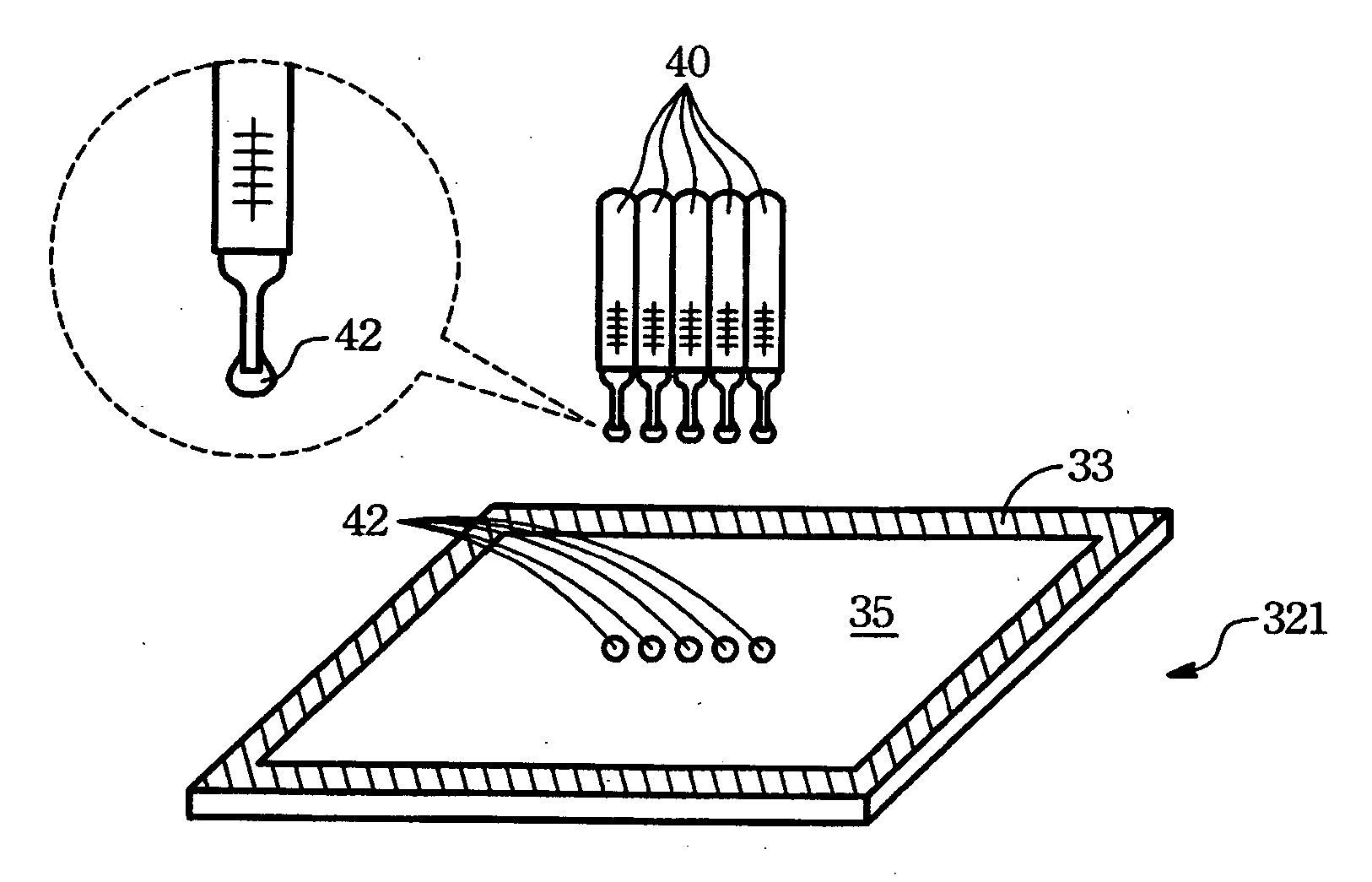
[0026] Please refer to FIG. 4A to FIG. 4D, which show four consecutive steps of a preferred ODF fabricating process of the present invention. The LCD panel herein comprises a first substrate 321 and a second substrate 323. Firstly, as FIG. 4A shows, an alignment layer 35 is applied onto the upper surface of the first substrate 321, which the alignment layer 35 is composed of PI and PAA. Then, a post baking process can be used to transfer the PAA into PI as the following formula:

[0027] The temperature of the post baking process is in a range between 180 degree centigrade and 240 degree centigrade.

[0028] Please refer to FIG. 4A, if the LCD panel is a TN-TFT mode, an IPS mode, or an OCB mode, a a step of rubbing to arrange the alignment layer 35 with a unique angle is followed. The a step of rubbing can be accomplished by mechanical rubbing, and have advantages of being operable under room temperature and less time consumption. In another embodiment of the LCD panel being a VA mode,...


PUM

PropertyMeasurementUnit
Fractionaaaaaaaaaa
Fractionaaaaaaaaaa
Fractionaaaaaaaaaa

Abstract

A method of manufacturing an LCD panel, which the LCD panel includes a first substrate and a second substrate, includes following steps of: 1) forming an alignment layer on the first and second substrates, the alignment layer comprising PI and PAA; 2) post baking to convert PAA into PI, wherein the imidization rate of the alignment layer after the post baking is between 70% and 90%; 3) spreading a sealant in the margin area of the first substrate; 4) dropping a liquid crystal material upon the first substrate; and 5) gluing the first substrate and the second substrate under a low-pressure condition.

Description

(1) FIELD OF THE INVENTION [0001] The present invention relates to a method for producing a liquid crystal panel, and more particularly to a one-drop-fill (ODF) method of manufacturing a liquid crystal panel. (2) DESCRIPTION OF THE PRIOR ART [0002] Liquid crystal display (LCD) panels are key elements of plan displays, In the LCD panel, liquid crystals are sealed, by a proper sealant, within two substrates. One of the two substrates comprises an electrode pixel array, which the electrode pixel forming the element of the electrode pixel array is used for controlling the spin angle of the liquid crystal molecules. The other substrate comprises a color filter used for presenting colorful images of the panel. [0003] Please refer to FIG. 1A, in which a set 12 of a pair of substrates integrated by a circling sealant 13 is positioned in a vacuum chamber 10. The substrate set 12 comprises a first substrate 121 and a second substrate 123, and one of the substrates 121 or 123 includes an elect...

Claims


Application Information

Patent Timeline
IPC IPC(8): G02F1/13
CPCG02F1/133723G02F1/133784G02F1/1339G02F1/1341G02F2001/13415G02F1/13415
Inventor CHEN, TE-SHENGYANG, KAI-NENGTAI, CHIA-HSUAN
Owner AU OPTRONICS CORP
Why Eureka
Try Eureka