Image defect inspection method, image defect inspection apparatus, and appearance inspection apparatus

a technology of defect detection and inspection method, applied in the direction of image enhancement, image analysis, instruments, etc., can solve the problems of reducing detection sensitivity, excessively large or excessively small threshold value, and affecting the detection effect of defects

Inactive Publication Date: 2006-07-20
TOKYO SEIMITSU
View PDF5 Cites 54 Cited by
  • Summary
  • Abstract
  • Description
  • Claims
  • Application Information

AI Technical Summary

Problems solved by technology

However, the method disclosed in the above cited Japanese Unexamined Patent Publication No. 2004-177397 has had the problem that, if the distribution of the gray level difference of the electrical image signal greatly differs from the prescribed type of distribution assumed when computing the converted cumulative frequency, the converted cumulative frequency thus computed does not become linear, and there arises the possibility that the threshold value may be set excessively large or excessively small.
This means that the number of pixels to be detected as defective becomes excessively small, that is, the detection sensitivity drops because the threshold value is set too high.

Method used


Image

  • Image defect inspection method, image defect inspection apparatus, and appearance inspection apparatus
  • Image defect inspection method, image defect inspection apparatus, and appearance inspection apparatus
  • Image defect inspection method, image defect inspection apparatus, and appearance inspection apparatus

Examples


Embodiment Construction

[0048] Preferred embodiments of the present invention will be described in detail below while referring to the attached drawings.

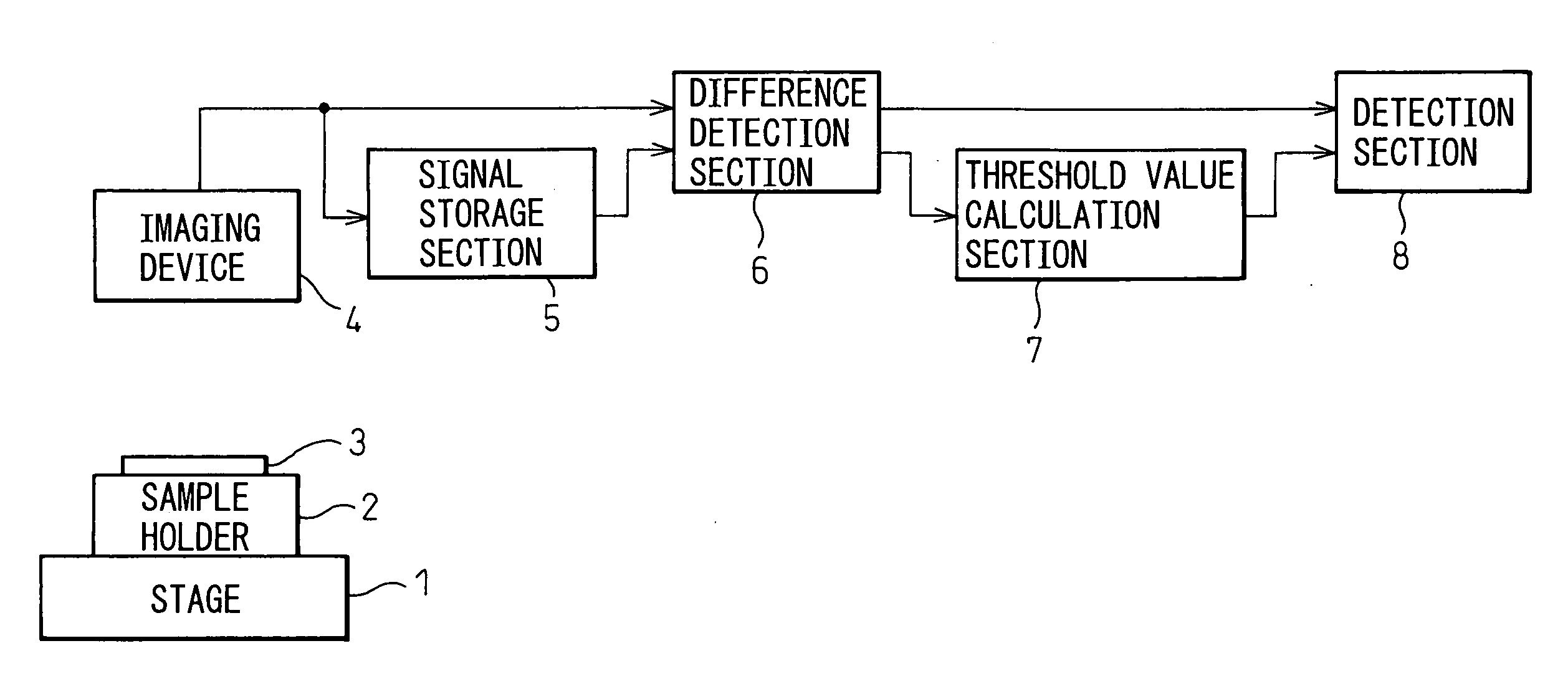
[0049]FIG. 3 is a block diagram showing the general configuration of a semiconductor pattern appearance inspection apparatus according to a first embodiment of the present invention. As shown, a sample holder (chuck stage) 2 is installed on the upper surface of a stage 1 which is freely movable in two- or three-dimensional directions. A semiconductor wafer 3 to be inspected is mounted and held fixed onto the sample holder 2. An imaging device 4 comprising a one-dimensional or a two-dimensional CCD camera or the like is disposed above the stage, and the imaging device 4 generates an image signal by capturing an image of a pattern formed on the semiconductor wafer 3.

[0050] As shown in FIG. 4, a plurality of dies 3a are formed on the semiconductor wafer 3 in a matrix pattern repeating in X and Y directions. As the same pattern is formed on each die, it is g...


PUM


Abstract

In an image defect inspection method and apparatus which detects a gray level difference between corresponding portions of two images, automatically sets a threshold value based on the distribution thereof, compares the gray level difference with the threshold value, and judges one or the other of the portions to be defective if the gray level difference is larger than the threshold value, provisions are made to correct the threshold value when the distribution of the gray level difference is different from the usual distribution, thereby achieving high detection sensitivity while suppressing the occurrence of false defects. To achieve this object, the cumulative frequency of the gray level difference is computed (S3); a converted cumulative frequency is computed by converting the cumulative frequency so that the cumulative frequency shows a linear relationship with respect to the gray level difference when the gray level difference is assumed to exhibit a distribution that obeys a prescribed type of distribution (S4); an approximation curve of the converted cumulative frequency is derived (S11); the second derivative of the approximation curve with respect to the gray level difference is computed (S12); and the threshold value is corrected in accordance with the second derivative (S13).

Description

BACKGROUND OF THE INVENTION [0001] 1. Field of the Invention [0002] The present invention relates to a defect inspection method and apparatus which detects a difference between corresponding signals, compares the detected difference with a threshold value, and judges the part under inspection to be defective if the difference is larger than the threshold value. More particularly, the invention relates to an image defect inspection method and apparatus which detects a gray level difference between corresponding portions of two images, compares the detected gray level difference with a threshold value, and judges the part under inspection to be defective if the gray level difference is larger than the threshold value; the invention also relates to an appearance inspection apparatus which, by using such a method, detects a defect in a semiconductor circuit pattern formed on a semiconductor wafer. Still more particularly, the present invention relates to a technique for correcting the a...

Claims


Application Information

Patent Timeline
Patent Type & Authority Applications(United States)
IPC IPC(8): G06K9/00
CPCG06T7/001G06T2207/30148
Inventor ISHIKAWA, AKIO
Owner TOKYO SEIMITSU
Why Eureka
Try Eureka