Tag writing and reading method for semiconductor product

a technology for semiconductor products and writing methods, applied in the field of tag writing and reading methods for semiconductor products, can solve the problems that identification cannot be readily tampered to protect designers and manufacturers, and achieve the effect of not easily tampered, easy identification, and easy tampering

Inactive Publication Date: 2006-08-31
UNITED MICROELECTRONICS CORP
View PDF6 Cites 2 Cited by
  • Summary
  • Abstract
  • Description
  • Claims
  • Application Information

AI Technical Summary

Benefits of technology

[0012] Accordingly, in the tag writing method of the present invention, the tag is coded and then converted into a tag pattern, and then the tag pattern is combined with the pattern of the IC. Since the tag pattern and the circuit pattern are combined, they can not easily identified and readily tampered by any unauthorized persons. In the tag reading method of the present invention, the information of the tag is read according to a predetermined principle. Compared to the conventional tagging method, the present invention provides a tag for product identification that can not be easily tampered.

Problems solved by technology

Therefore, it is highly desirable that a tag serving as product identification can not be readily tampered to safe guard designers and manufacturers.

Method used


Image

  • Tag writing and reading method for semiconductor product
  • Tag writing and reading method for semiconductor product
  • Tag writing and reading method for semiconductor product

Examples


Embodiment Construction

[0023] The present invention now will be described more fully hereinafter with reference to the accompanying drawings, in which embodiments of the invention are shown. This invention may, however, be embodied in many different forms and should not be construed as limited to the embodiments set forth herein; rather, these embodiments are provided so that this disclosure will be thorough and complete, and will fully convey the scope of the invention to those skilled in the art. Like numbers refer to like elements throughout.

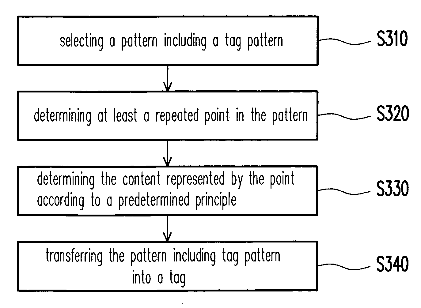
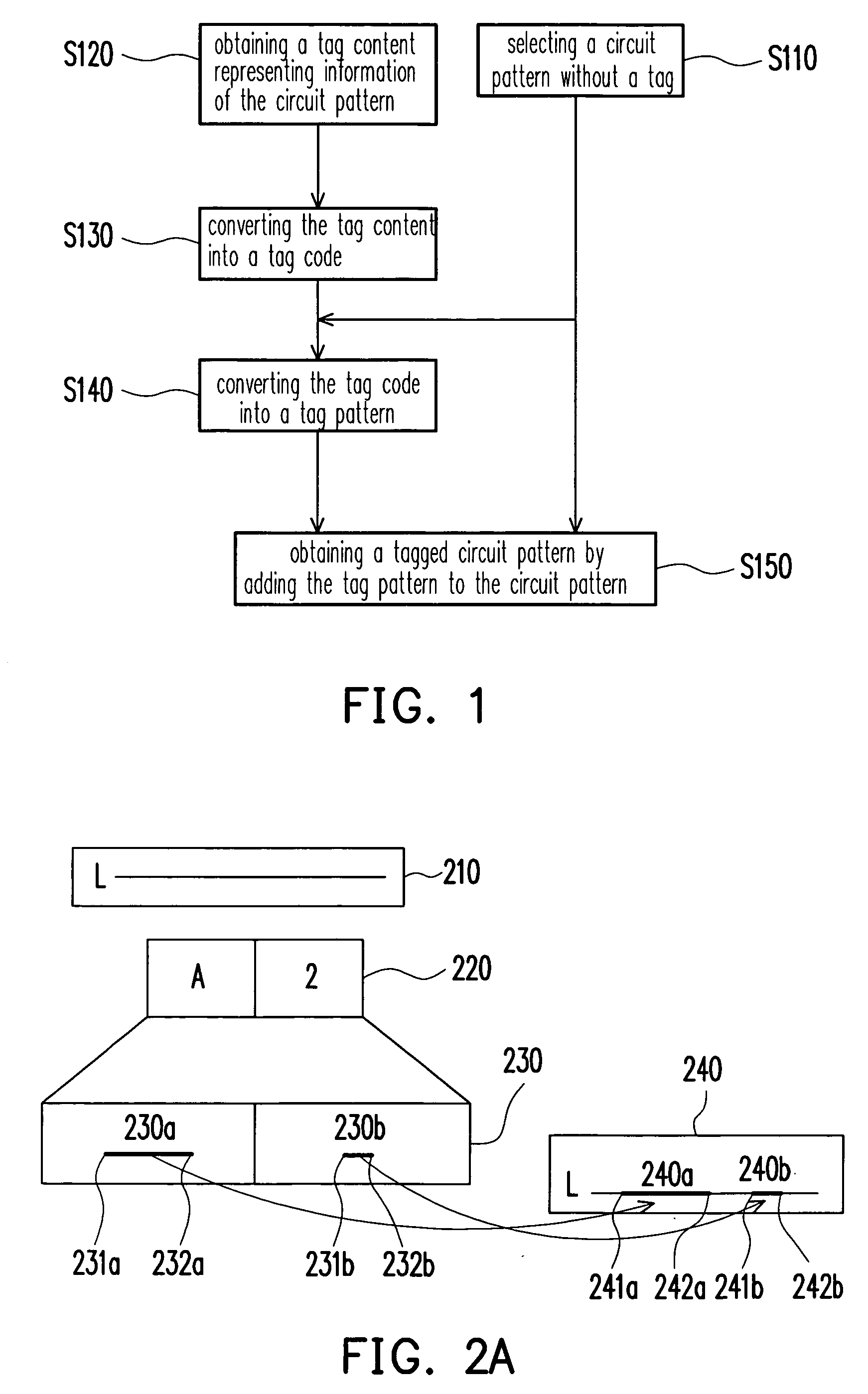
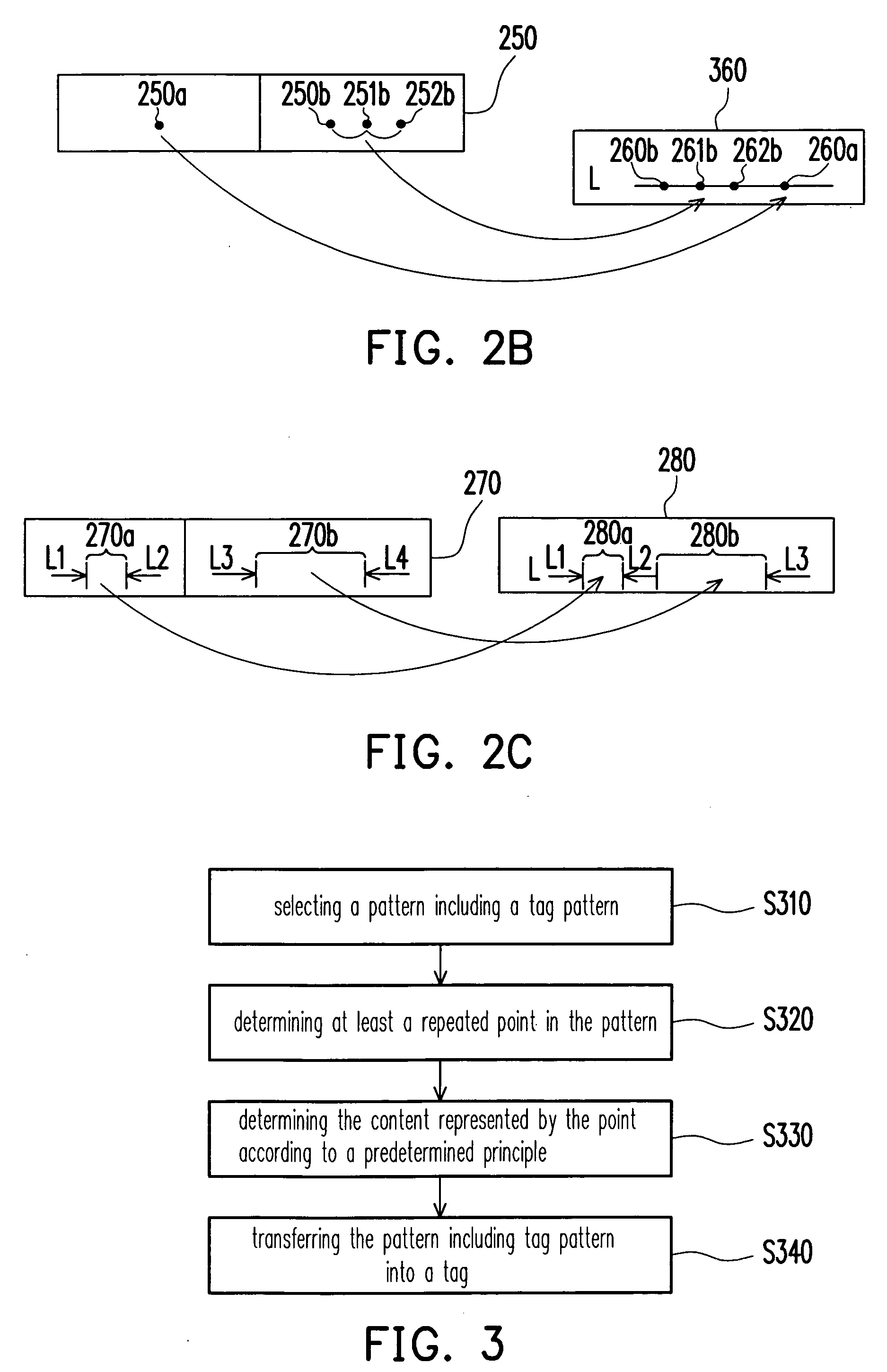
[0024]FIG. 1 is a flowchart of a tag writing method for a semiconductor product according to one embodiment of the present invention. Referring to FIG. 1, at step S110, a circuit pattern without a tag is selected. At step S120, a tag content representing information of the circuit pattern is obtained. It is noted that the term “circuit pattern” will be referred to the “circuit pattern without any tag”. Thereafter, at step S130, the tag content is converted into a ...


PUM


Abstract

A tag writing and reading method suitable for a semiconductor product are provided. In the tag writing method, a code representing a tag is provided, and then the code is converted into a tag pattern that is then combined with a portion of the pattern of the pattern. Next, the pattern is combined with the tag pattern and used as the design content of the semiconductor product. In addition, a length of line segment, a number of points or interval(s) between a plurality of line segments may be adopted for representing the code of the tag. In addition, the tag code may include a patent number.

Description

BACKGROUND OF THE INVENTION [0001] 1. Field of the Invention [0002] The present invention generally relates to a tag writing and reading method. More particularly, the present invention relates to a tag writing and reading method for a semiconductor product. [0003] 2. Description of Related Art [0004] Conventionally, tag is usually adopted for tagging information of goods. In recent years, the tag is also being applied in a variety of semiconductor products information related to, for example, a pattern of an integrated circuit (IC). In general, some useful information such as product name, product version, design date, design place, or test parameter may be tagged as the design pattern of the products for the identification of the pattern. [0005] Furthermore, along with the advance of concept of knowledge property, information on the tags of the patterns of the products should not be arbitrarily modified by anyone else other than the concerned factories, which information is adopte...

Claims


Application Information

Patent Timeline
Patent Type & Authority Applications(United States)
IPC IPC(8): G06F17/00
CPCG06K19/10
Inventor HUANG, RANDYKUO, ANDREWCHUI, JASONHSU, BRIAN CC.FENG, TINA
Owner UNITED MICROELECTRONICS CORP
Why Eureka
Try Eureka