Emitter, manufacturing method and manufacturing apparatus thereof, electro-optical apparatus and electronic apparatus
a manufacturing method and technology of emitter, applied in the direction of discharge tube/lamp details, electroluminescent light sources, organic semiconductor devices, etc., can solve the problems of white balance breakdown and inability to obtain the intended emitted color, and achieve the effect of small deterioration over tim
- Summary
- Abstract
- Description
- Claims
- Application Information
AI Technical Summary
Benefits of technology
Problems solved by technology
Method used
Image
Examples
first embodiment
[0040] First, an explanation is provided of a manufacturing apparatus for producing an EL apparatus.
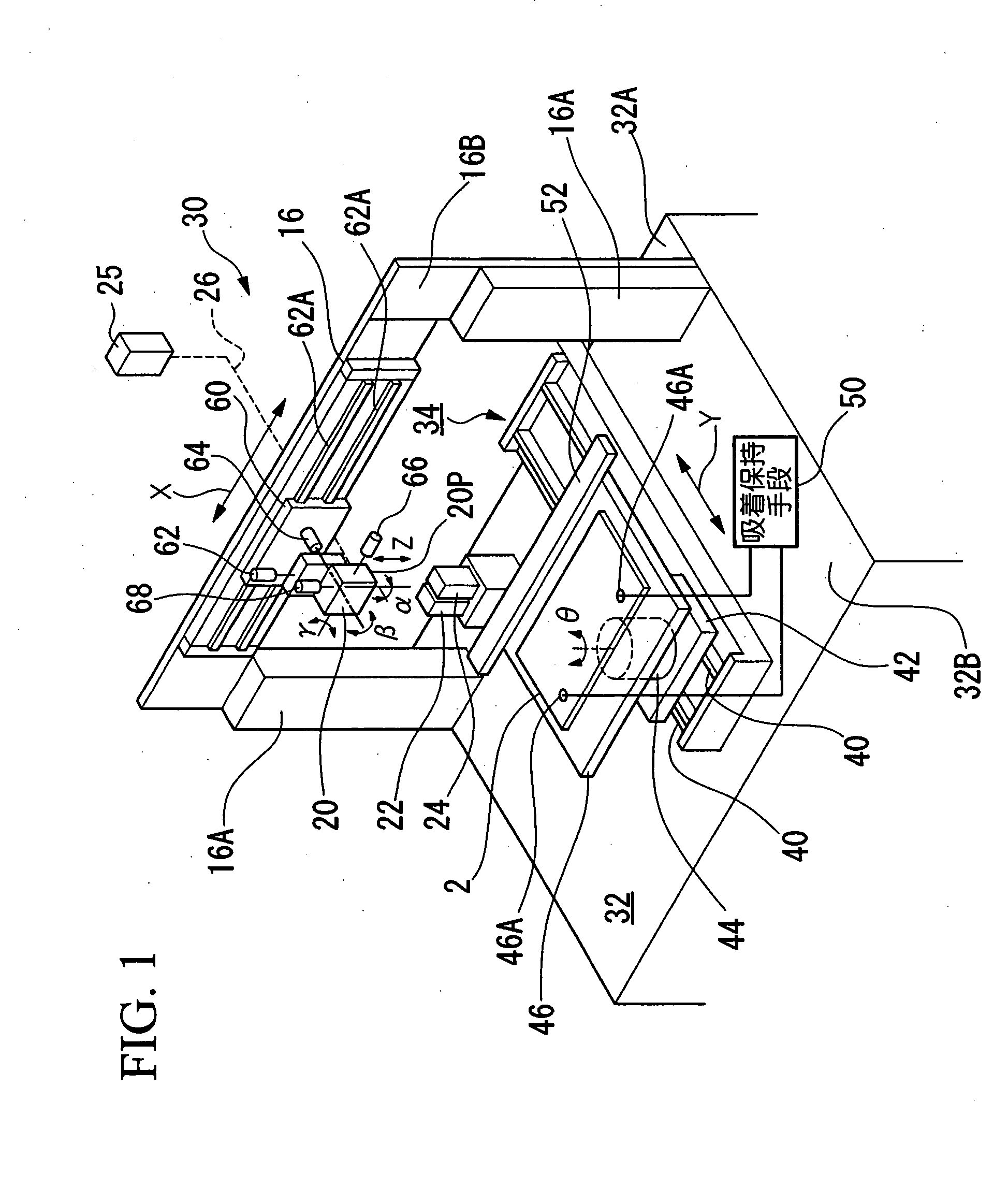
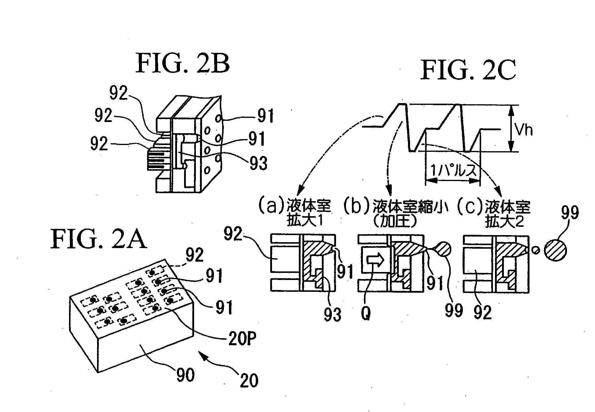
[0041]FIG. 1 is a perspective view of the general appearance of a film deposition apparatus (inkjet apparatus) that composes an EL manufacturing apparatus (device manufacturing apparatus). Film deposition apparatus 30 employs a constitution in which an ink to be described later containing light-emitting materials and a positive hole transport material is discharged onto a substrate by an inkjet system.
[0042] Film deposition apparatus 30 has, among other components, a base 32, a first movement unit 34, a second movement unit 16, an electronic balance not shown (weighing unit), a liquid droplet discharge head in the form of inkjet head (discharge apparatus) 20, a capping unit 22 and a cleaning unit 24. The first movement unit 34, electronic balance, capping unit 22, cleaning unit 24 and second movement unit 16 are respectively arranged on base 32.
[0043] First movement unit 34 is pref...
example
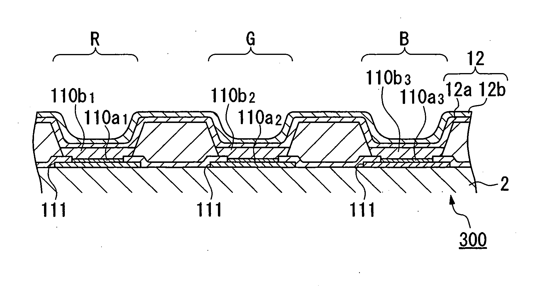
[0108] a. Positive hole transport layer materials were printed at 10 ng×10 shots onto pixels surrounded by bank sections for R (red), G (green) and B (blue) pixels, respectively. As a result, the film thickness of the R, G and B pixels was 60 nm each.
[0109] b. A light-emitting layer (organic EL layer) was deposited on the R, G and B pixels, respectively, at 80 nm while in this state followed by the deposition of a cathode thereon by vacuum vapor deposition to obtain a light-emitting device.
[0110] c. As a result of measuring the service life of this device, the service half-lives of R, G and B were 1800 h for R, 3000 h for G and 1000 h for B. However, the time during which white color was obtained was 700 h due to a shift in color balance during white display.
[0111] d. Next, liquid droplets of a positive hole transport layer forming material were discharged onto the pixels surrounded by bank sections at 10 ng×8 shots for the R pixel, 10 ng×6 shots for the G pixel, and 10 ng×10 sho...
second embodiment
[0115]FIG. 9 is a perspective view showing a mobile personal computer as an example of electronic apparatus equipped with an organic EL apparatus (emitter) of the present invention.
[0116] Mobile personal computer 200 is provided with a main unit 202 equipped with a keyboard 201, and a display unit 203 composed of an organic EL apparatus (emitter) according to the aforementioned first embodiment.
PUM
 Abstract
Description
Claims
Application Information


