Emitter, manufacturing method and manufacturing apparatus thereof, electro-optical apparatus and electronic apparatus

a manufacturing method and technology of emitter, applied in the direction of discharge tube/lamp details, organic semiconductor devices, thermoelectric devices, etc., can solve the problems of white balance breakdown and inability to obtain the intended emitted color, and achieve the effect of small deterioration over tim

Inactive Publication Date: 2006-07-04
SEIKO EPSON CORP
View PDF6 Cites 5 Cited by
  • Summary
  • Abstract
  • Description
  • Claims
  • Application Information

AI Technical Summary

Benefits of technology

[0011]According to this aspect, by adjusting the deterioration of emission characteristics over time in a predetermined type of light-emitting unit to match the deterioration over time in another light-emitting unit, the state of deterioration between the plurality of types of light-emitting units can be made to be the same even if changes in emission characteristics occur over time, thereby making it possible to maintain a constant color balance by the plurality of types of light-emitting units.
[0025]In this case, by adjusting the weight or number of drops of the liquid discharged, for example, a hole donor can be thinly formed in a predetermined type of light-emitting unit having a small degree of deterioration over time.

Problems solved by technology

However, conventionally, there are problems like those described below.
Although a product is able to maintain satisfactory white balance immediately after being shipped, due to differences in the deterioration characteristics of the red, green and blue light-emitting materials over time, the white balance breaks down due to changes in each color over time.
Thus, even when a predetermined current is supplied to each organic EL device with the intention of emitting white light, the actual color is not an attractive white color, and even if another arbitrary color is attempted to be emitted at an arbitrary brightness, there was the problem of again not being able to obtain the intended emitted color.

Method used


Image

  • Emitter, manufacturing method and manufacturing apparatus thereof, electro-optical apparatus and electronic apparatus
  • Emitter, manufacturing method and manufacturing apparatus thereof, electro-optical apparatus and electronic apparatus
  • Emitter, manufacturing method and manufacturing apparatus thereof, electro-optical apparatus and electronic apparatus

Examples


first embodiment

[0039]First, an explanation is provided of a manufacturing apparatus for producing an EL apparatus.

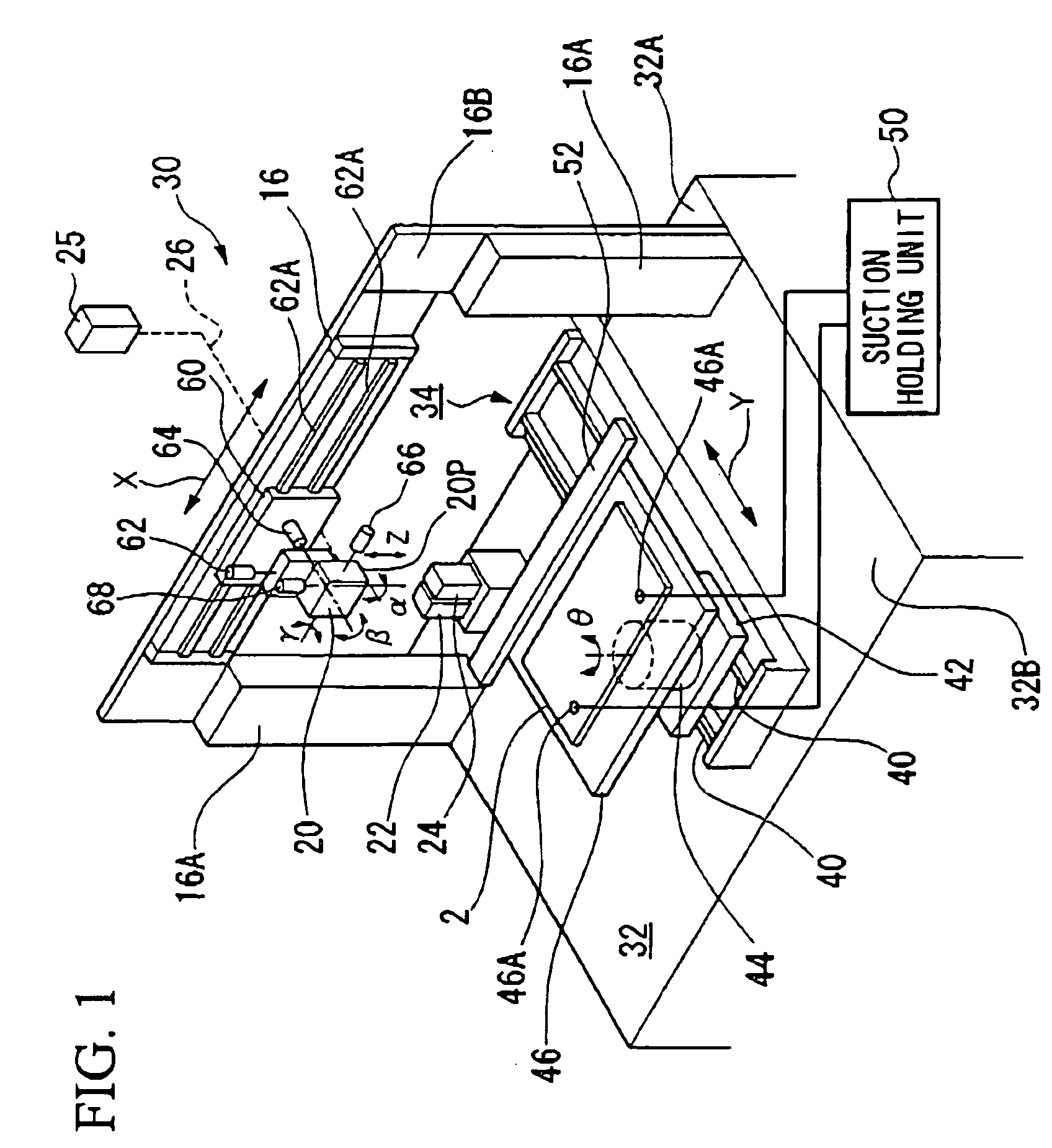
[0040]FIG. 1 is a perspective view of the general appearance of a film deposition apparatus (inkjet apparatus) that composes an EL manufacturing apparatus (device manufacturing apparatus). Film deposition apparatus 30 employs a constitution in which an ink to be described later containing light-emitting materials and a positive hole transport material is discharged onto a substrate by an inkjet system.

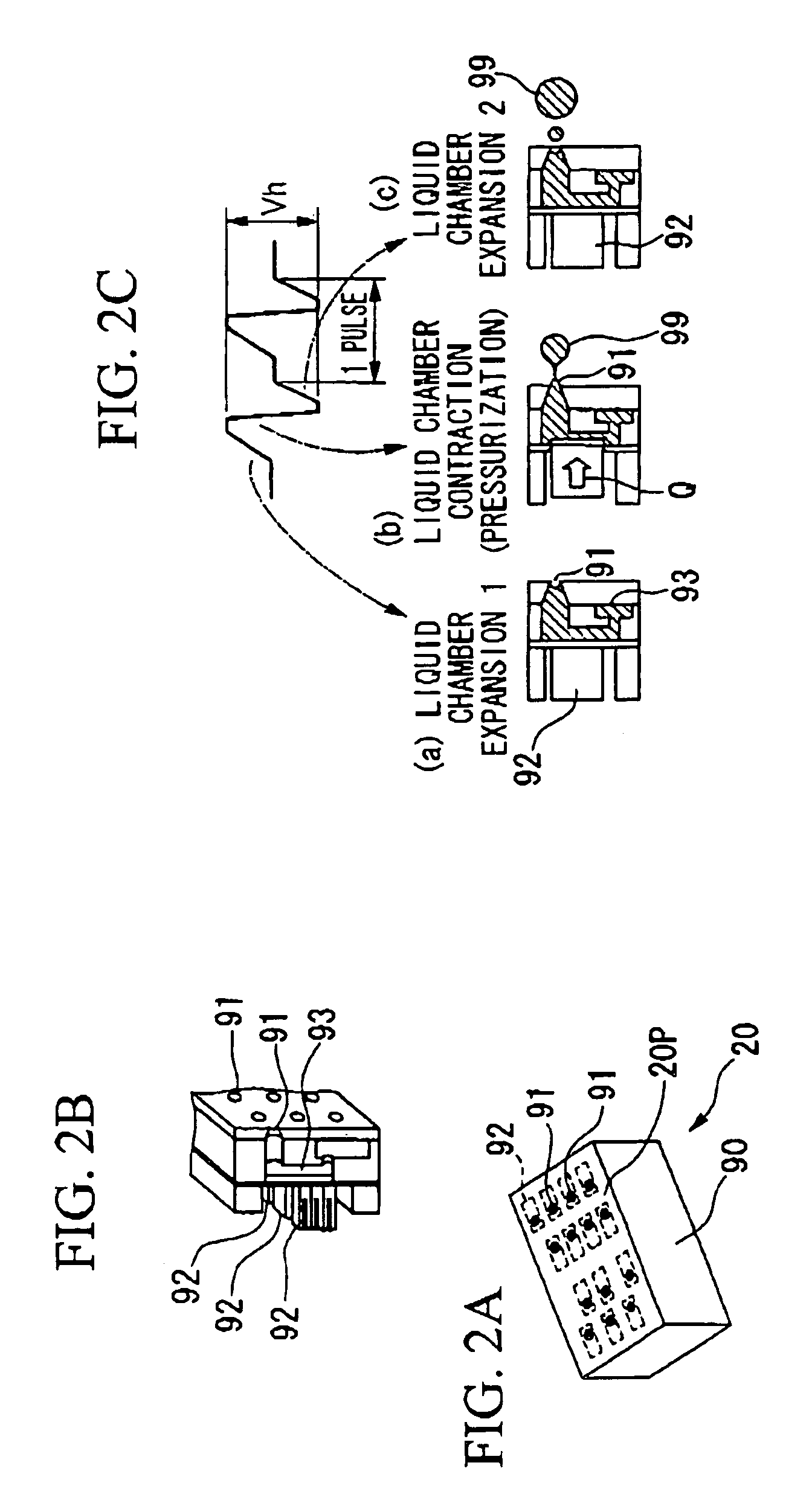
[0041]Film deposition apparatus 30 has, among other components, a base 32, a first movement unit 34, a second movement unit 16, an electronic balance not shown (weighing unit), a liquid droplet discharge head in the form of inkjet head (discharge apparatus) 20, a capping unit 22 and a cleaning unit 24. The first movement unit 34, electronic balance, capping unit 22, cleaning unit 24 and second movement unit 16 are respectively arranged on base 32.

[0042]First movement unit 34 is preferably...

example

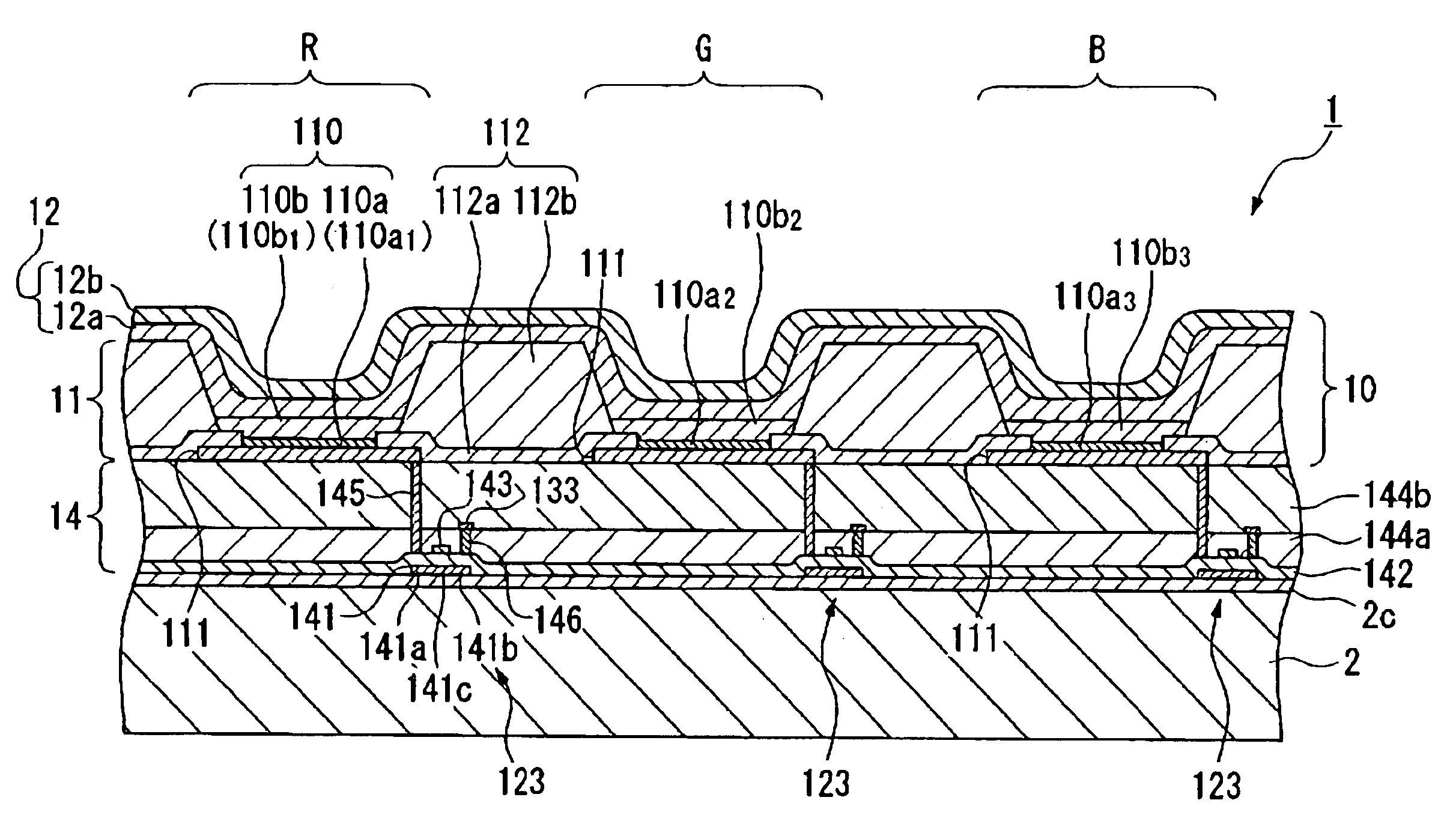
[0107](1) Positive hole transport layer materials were printed at 10 ng×10 shots onto pixels surrounded by bank sections for R (red), G (green) and B (blue) pixels, respectively. As a result, the film thickness of the R, G and B pixels was 60 nm each.[0108](2) A light-emitting layer (organic EL layer) was deposited on the R, G and B pixels, respectively, at 80 nm while in this state followed by the deposition of a cathode thereon by vacuum vapor deposition to obtain a light emitting device.[0109](3) As a result of measuring the service life of this device, the service half-lives of R, G and B were 1800 h for R, 3000 h for G and 1000 h for B. However, the time during which white color was obtained was 700 h due to a shift in color balance during white display.[0110](4) Next, liquid droplets of a positive hole transport layer forming material were discharged onto the pixels surrounded by bank sections at 10 ng×8 shots for the R pixel, 10 ng×6 shots for the G pixel, and 10 ng×10 shots ...

second embodiment

[0114]FIG. 9 is a perspective view showing a mobile personal computer as an example of electronic apparatus equipped with an organic EL apparatus (emitter) of the present invention.

[0115]Mobile personal computer 200 is provided with a main unit 202 equipped with a keyboard 201, and a display unit 203 composed of an organic EL apparatus (emitter) according to the aforementioned first embodiment.

THRID EMBODIMENT

[0116]FIG. 10 is a perspective view showing a cell phone as an example of electronic apparatus equipped with an organic EL apparatus (emitter) of the present invention.

[0117]Mobile telephone 300 is provided with a plurality of operating buttons 301, an earpiece 302, a mouthpiece 303 and an organic EL apparatus (emitter) 304 according to the aforementioned first embodiment.


PUM


Abstract

An emitter has a plurality of types of light-emitting units with different changes in emission characteristics over time. In addition, the emitter includes a deterioration adjustment device which adjusts the deterioration of the emission characteristics over time in a predetermined type of light-emitting unit. The light-emitting units respectively include a light-emitting layer and a hole donor which supplies positive holes to the light-emitting layer, and the deterioration adjustment device may be the hole donor in which the thickness is adjusted based on the deterioration in emission characteristics over time in the predetermined type of light-emitting unit.

Description

BACKGROUND OF THE INVENTION[0001]1. Field of the Invention[0002]The present invention relates to an emitter, a manufacturing method and a manufacturing apparatus thereof, an electro-optical apparatus and an electronic apparatus.[0003]2. Description of Related Art[0004]Various emitters such as displays and light sources using self-emitting devices in the form EL devices (and particularly organic EL devices) have been proposed in the past, and among these emitters, an organic EL display apparatus is also known that is capable of displaying colors. During the production of an organic EL device, for example, a material that forms a light-emitting layer and a material that forms a positive hole injection (PEDOT) / electron transport layer are used as ink, and each material is patterned on a device substrate such as a TFT by red, green and blue ink using an inkjet method to produce a self-emitting full-color EL device, and this technology is disclosed in Japanese Unexamined Patent Applicati...

Claims


Application Information

Patent Timeline
Patent Type & Authority Patents(United States)
IPC IPC(8): H01L35/24H01L51/50H01J1/00H01L27/32H01L51/00H01L51/52H05B33/10H05B33/14H05B33/22H05B33/26
CPCH01L27/3211H01L51/0005H01L27/3244H01L27/3295H01L2251/558H01L51/5048H01L51/5092H01L51/5221H10K59/35H10K71/135H10K59/122H10K59/12H10K50/14H10K50/171H10K50/828H10K2102/351H05B33/10
Inventor SAKAI, HIROFUMI
Owner SEIKO EPSON CORP
Why Eureka
Try Eureka