Automatic detection method and system for chip surface defects and electronic equipment

An automatic detection and surface defect technology, which is applied in the direction of optical test defect/defect, measurement device, image data processing, etc., can solve the problems of low accuracy, low detection precision, slow detection speed, etc., and achieve the effect of improving the detection speed

Pending Publication Date: 2021-02-02
WUHAN INSTITUTE OF TECHNOLOGY
View PDF0 Cites 5 Cited by
  • Summary
  • Abstract
  • Description
  • Claims
  • Application Information

AI Technical Summary

Problems solved by technology

[0005] In order to overcome the problems of low accuracy, low detection precision and slow detection speed in the exi

Method used


Image

  • Automatic detection method and system for chip surface defects and electronic equipment
  • Automatic detection method and system for chip surface defects and electronic equipment
  • Automatic detection method and system for chip surface defects and electronic equipment

Examples


Embodiment Construction

[0059] The following examples are further explanations and supplements to the present invention, and do not constitute any limitation to the present invention.

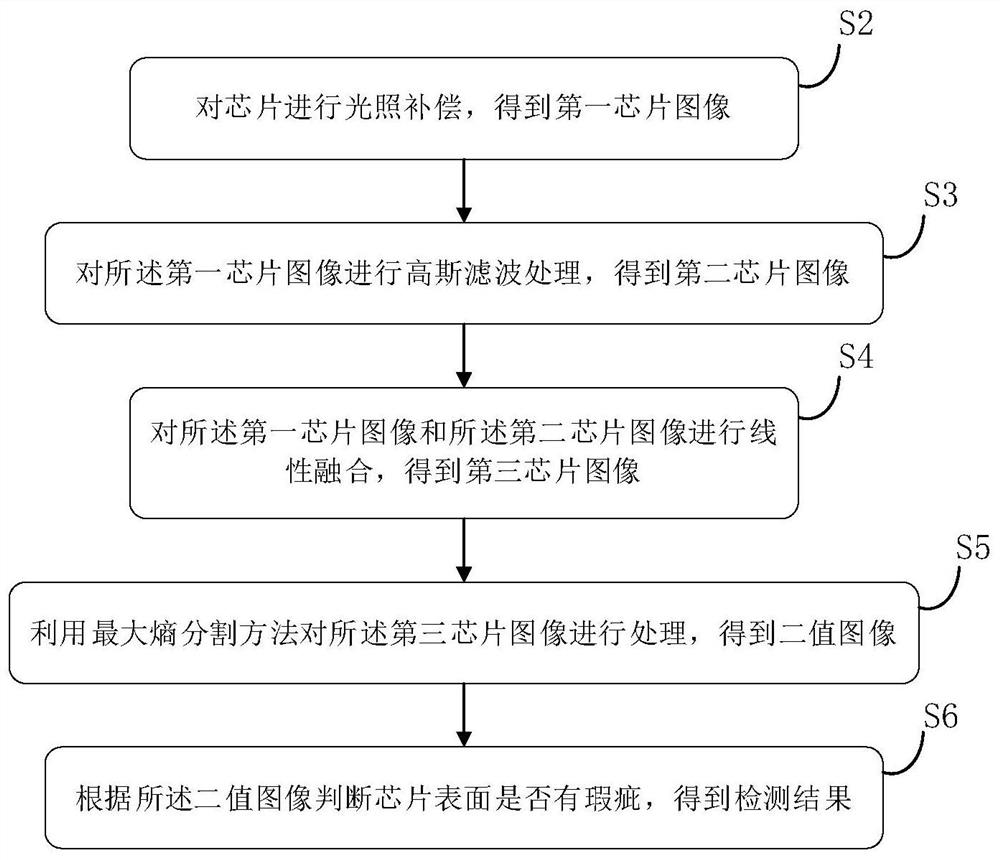
[0060] Such as figure 1 Shown, the embodiment of the automatic detection method of a kind of chip surface blemish of the present invention, comprises the following steps:

[0061] S2. Perform light compensation on the chip image to obtain the first chip image;

[0062] S3. Perform Gaussian filter processing on the first chip image to obtain a second chip image;

[0063] S4. Perform linear fusion on the first chip image and the second chip image to obtain a third chip image;

[0064] S5. Using a maximum entropy segmentation method to process the image of the third chip to obtain a binary image;

[0065] S6. Determine whether there is a defect on the surface of the chip according to the binary image, and obtain a detection result.

[0066] Illumination compensation for the image can correct the uneven illumination p...


PUM


Abstract

The invention relates to an automatic detection method and system for chip surface defects and electronic equipment, and the method comprises the steps: carrying out illumination compensation of a chip image to acquire a first chip image; performing Gaussian filtering on the first chip image to obtain a second chip image; performing linear fusion on the first chip image and the second chip image to obtain a third chip image; processing the third chip image by using a maximum entropy segmentation method to obtain a binary image; and judging whether the surface of the chip has flaws or not according to the binary image to obtain a detection result. Therefore, the detection of the flaws on the surface of the chip is more intelligent and more convenient, and the efficiency of industrial production can be improved.

Description

technical field [0001] The invention relates to the fields of image processing and pattern recognition, in particular to an automatic detection method, system and electronic equipment for chip surface defects. Background technique [0002] The main task of chip detection in the chip production line is to use the image acquisition instrument to obtain the image of the chip and then pass it to the subsequent processing and identification unit to detect the defects on the chip surface, so as to determine whether the chip meets the production requirements. [0003] For the identification technology of chip surface defects, the current mainstream methods focus on various pre-processing of the chip to obtain better processing results. The commonly used deep learning method requires a huge sample size. At the same time, due to the imaging method of the image and the problem of the 16-bit image display, the image is huge, the image reasoning speed is slow, and a large amount of manu...

Claims


Application Information

Patent Timeline
IPC IPC(8): G06T7/00G06T7/12G06T7/13G06T7/136G06T7/194G01N21/88G01N21/95
CPCG01N21/8806G01N21/8851G01N21/95G01N2021/8858G01N2021/8874G01N2021/8887G06T7/0004G06T2207/20221G06T2207/30148G06T7/12G06T7/13G06T7/136G06T7/194
Inventor 曾祥进郑安义邓晨米勇宋彭彭
Owner WUHAN INSTITUTE OF TECHNOLOGY
Why Eureka
Try Eureka