Wafer strength reinforcement system for ultra thin wafer thinning

a technology of strength reinforcement and ultra thin wafer, which is applied in the direction of semiconductor devices, chemistry apparatus and processes, lamination ancillary operations, etc., can solve the problems of easy cracking, easy cracking of the wafer edge, and easy cracking of the wafer

Active Publication Date: 2006-10-05
STATS CHIPPAC LTD
View PDF17 Cites 28 Cited by
  • Summary
  • Abstract
  • Description
  • Claims
  • Application Information

AI Technical Summary

Problems solved by technology

However, these technologies can only reduce wafer stress within the wafer itself.
Hence, any application of uneven force during grinding or stress relieving can easily create a crack.
This crack can continue to spread during further handling and cause wafer edge chipping or even wafer cracking.
Because of the failure mechanism described, the existing wafer thinning technology will not able to provide a solution to prevent failures from occurring at the edge of the wafer.
Solutions to these problems have been long sought but prior developments have not taught or suggested any solutions and, thus, solutions to these problems have long eluded those skilled in the art.

Method used


Image

  • Wafer strength reinforcement system for ultra thin wafer thinning
  • Wafer strength reinforcement system for ultra thin wafer thinning
  • Wafer strength reinforcement system for ultra thin wafer thinning

Examples


Embodiment Construction

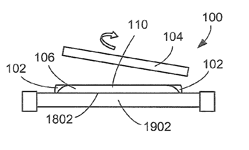
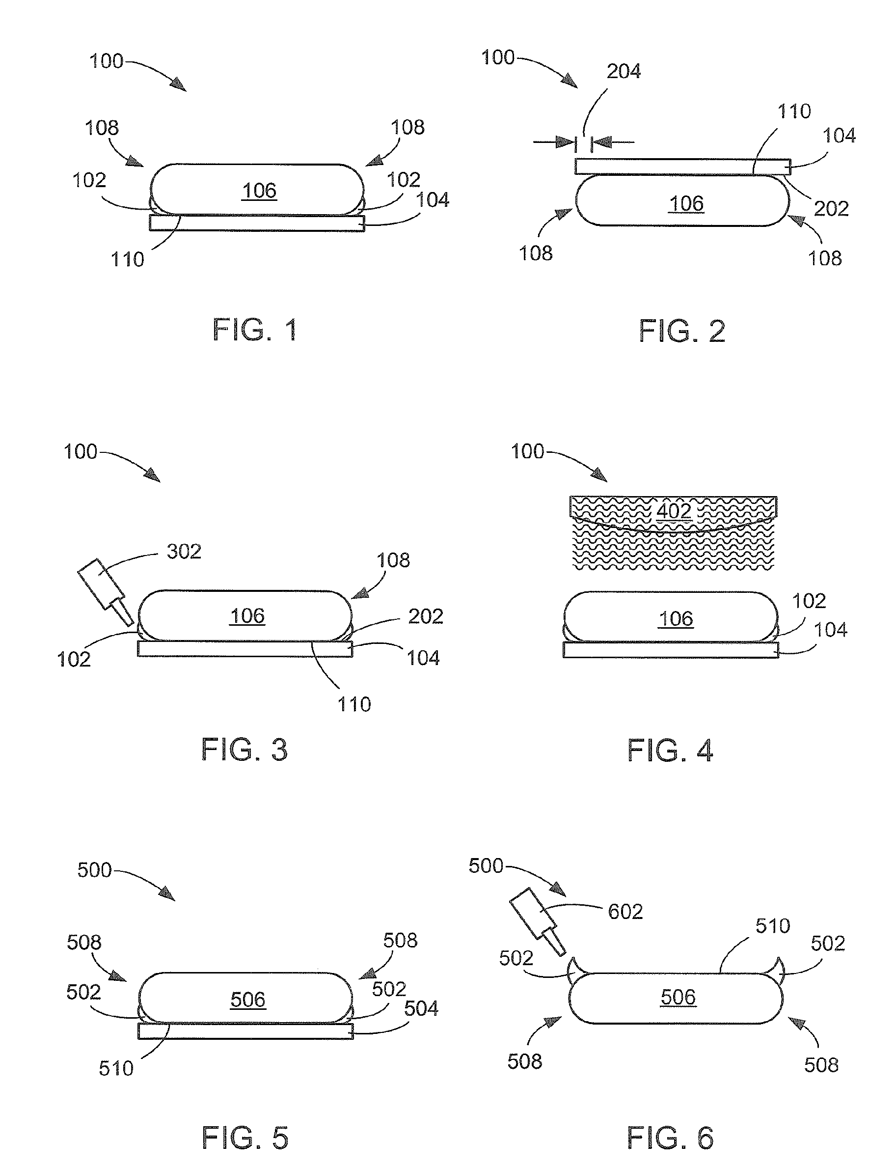
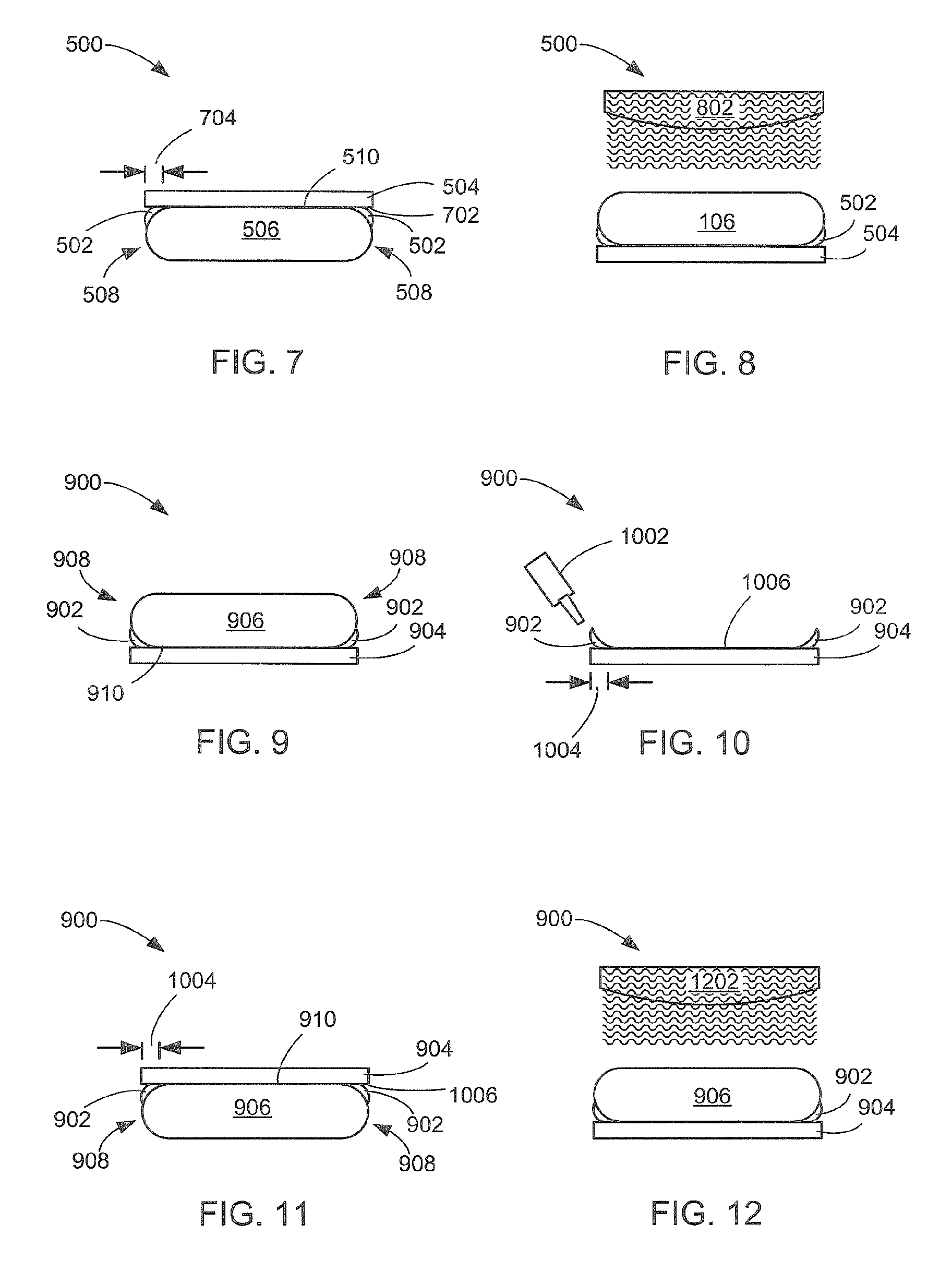
[0033] In the following description, numerous specific details are given to provide a thorough understanding of the invention. However, it will be apparent that the invention may be practiced without these specific details. In order to avoid obscuring the present invention, some well-known circuits, and process steps are not disclosed in detail.

[0034] Likewise, the drawings showing embodiments of the apparatus / device are semi-diagrammatic and not to scale and, particularly, some of the dimensions are for the clarity of presentation and are shown greatly exaggerated in the drawing FIGS. Similarly, although the sectional views in the drawings for ease of description show the invention with surfaces as oriented downward, this arrangement in the FIGS. is arbitrary and is not intended to suggest that invention should necessarily be in a downward direction. Generally, the device can be operated in any orientation. The same numbers are used in all the drawing FIGS. to relate to the same e...


PUM

PropertyMeasurementUnit
strengthaaaaaaaaaa
wafer strengthaaaaaaaaaa
sizeaaaaaaaaaa

Abstract

A wafer strength reinforcement system is provided including providing a wafer, providing a tape for supporting the wafer, and positioning a wafer edge support material for location between the tape and the wafer.

Description

CROSS-REFERENCE TO RELATED APPLICATION(S) [0001] This application claims the benefit of U.S. Provisional Patent Application Ser. No. 60 / 667,846 filed Apr. 2, 2005, and U.S. Provisional Patent Application Ser. No. 60 / 668,816 filed Apr. 5, 2005, and the subject matter thereof is hereby incorporated herein by reference thereto.TECHNICAL FIELD [0002] The present invention relates generally to ultra thin wafer thinning, and more particularly to a system for wafer strength reinforcement for ultra thin wafer thinning. BACKGROUND ART [0003] Integrated circuits are used in many portable electronic products, such as cell phones, portable computers, voice recorders, etc. as well as in many larger electronic systems, such as cars, planes, industrial control systems, etc. Across virtually all applications, there continues to be demand for reducing the size and increasing performance of the devices. The intense demand is no more visible than in portable electronics that have become so ubiquitous....

Claims


Application Information

Patent Timeline
Patent Type & Authority Applications(United States)
IPC IPC(8): B32B37/00B32B38/10B29C65/00H01L21/30H01L21/46
CPCH01L21/304H01L21/67132H01L21/3065H01L21/30604
Inventor KUAN, HEAP HOEDO, BYUNG TAI
Owner STATS CHIPPAC LTD
Why Eureka
Try Eureka