Eureka AIR delivers breakthrough ideas for toughest innovation challenges, trusted by R&D personnel around the world.

Lithographic apparatus and device manufacturing method utilizing multiple die designs on a substrate

a technology of die design and lithographic apparatus, which is applied in the direction of photomechanical equipment, instruments, optics, etc., can solve the problems of a large amount of data to define the pattern to be exposed on the substrate, complex process, and large cost of lithographic equipmen

Active Publication Date: 2006-10-05
ASML NETHERLANDS BV
View PDF23 Cites 38 Cited by
  • Summary
  • Abstract
  • Description
  • Claims
  • Application Information

AI Technical Summary

Benefits of technology

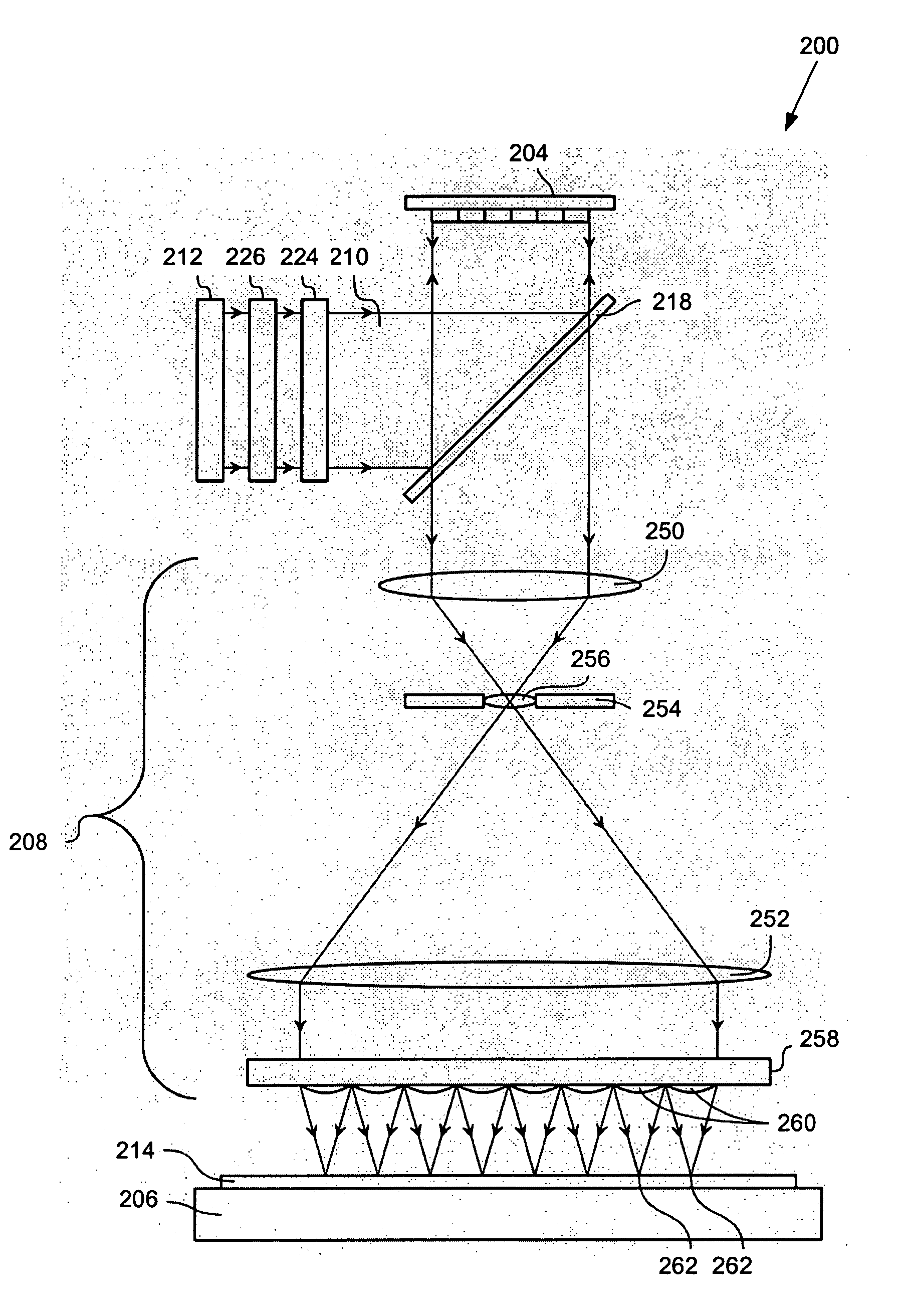
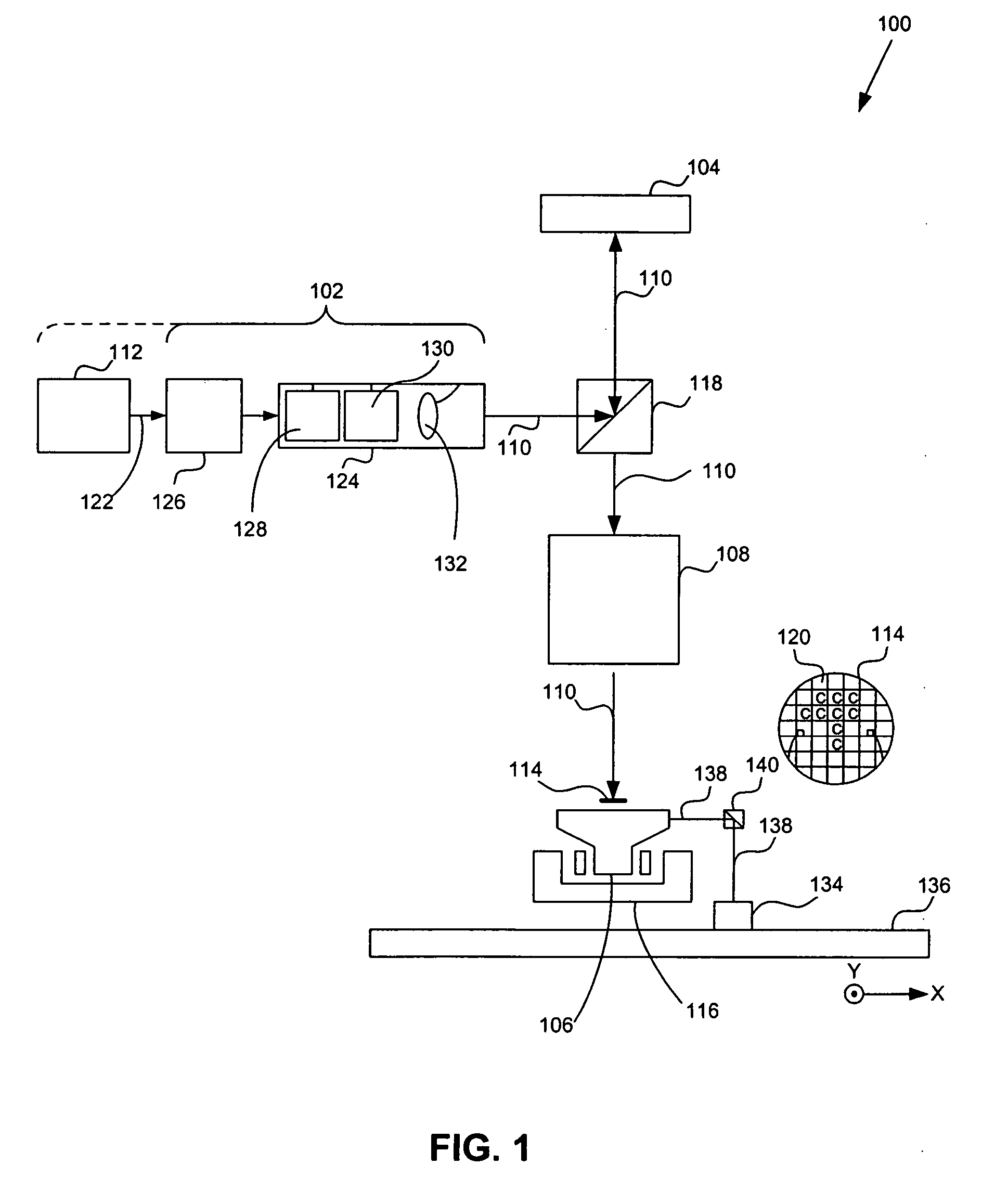
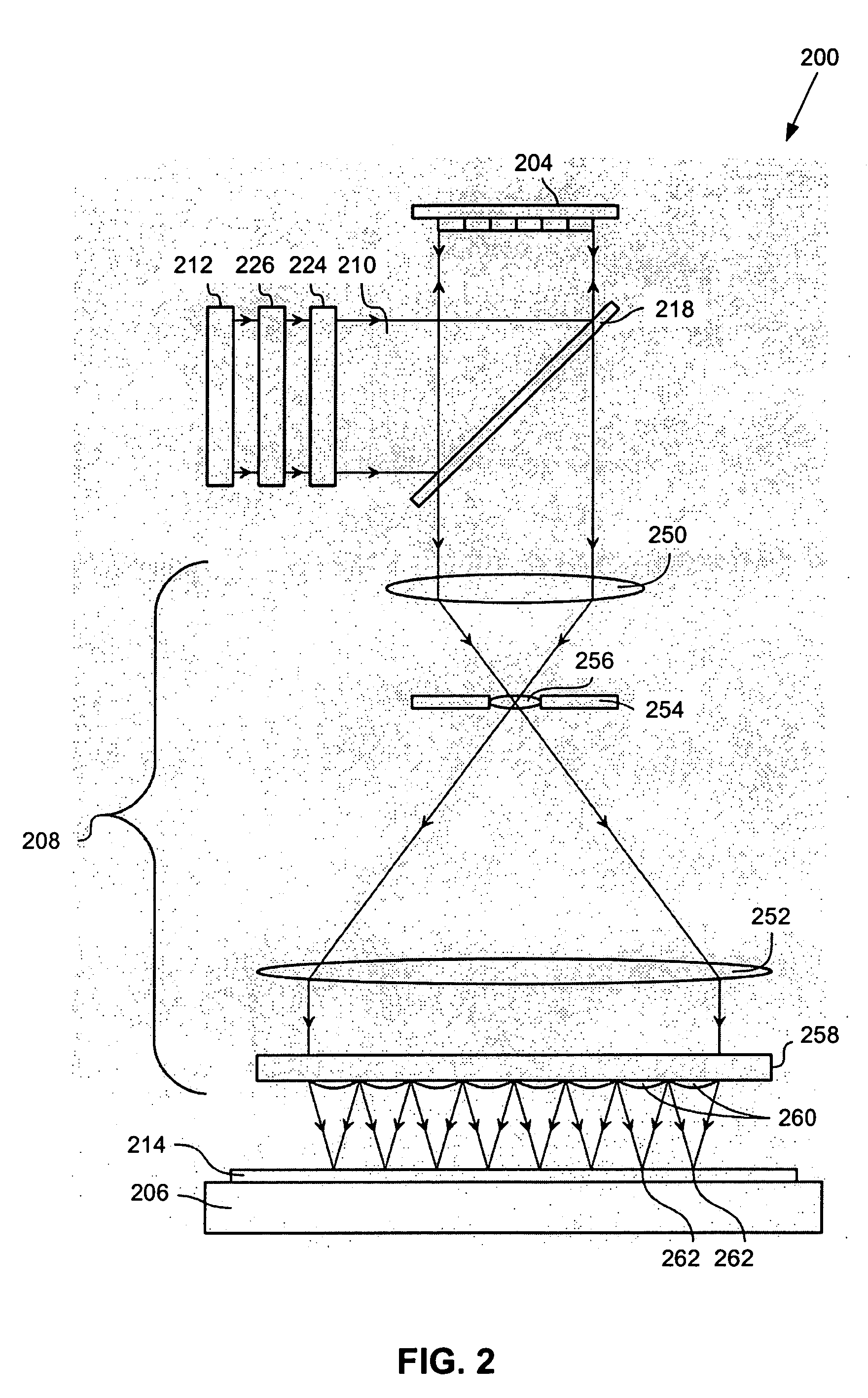
[0013] According to one embodiment of the present invention, there is provided a lithographic apparatus comprising an array of individually controllable elements, a control system, a first data buffer, and a second data buffer. The control system provides control signals to the array of individually controllable elements. The first data buffer stores pattern data that corresponds to a pattern to be exposed on a plurality of areas on the substrate. The second data buffer stores pattern variation data, corresponding to at least one change to a part of the pattern. The control system is configured such that at least one variation of the pattern is exposed on one of the areas on the substrate with the pattern variation data.

Problems solved by technology

In one example, the amount of data to define the pattern to be exposed on the substrate can be very large.
This process, commonly referred to as ‘rasterization,’ is complicated and the rasterizer represents a significant portion of the cost of the lithographic apparatus.
However, in order to achieve this cost saving, the apparatus is limited to providing a plurality of identical patterns on the substrate.

Method used


Image

  • Lithographic apparatus and device manufacturing method utilizing multiple die designs on a substrate
  • Lithographic apparatus and device manufacturing method utilizing multiple die designs on a substrate
  • Lithographic apparatus and device manufacturing method utilizing multiple die designs on a substrate

Examples


Embodiment Construction

Overview and Terminology

[0024] The use of “object,”“substrate,”“work piece,” or the like are interchangeable in this application, and can be, but are not limited to, a work piece, a substrate (e.g., a flat panel display glass substrate), a wafer (e.g., a semiconductor wafer for integrated circuit manufacture), a print head, micro or nano-fluidic devices, a display panel in a projection display system, or the like.

[0025] The terms “contrast device,”“patterning device,”“patterning array,” or “array of individually controllable elements” used herein should be broadly interpreted as referring to any device that can be used to modulate the cross-section of a radiation beam such as to create a pattern in a target portion of a substrate (e.g., object). It should be noted that the pattern imparted to the radiation beam may not exactly correspond to the desired pattern in the target portion of the substrate, for example if the pattern includes phase-shifting features or so called assist f...


PUM


Abstract

A lithographic system in which multiple variations of a basic device design can be generated without substantially increasing the cost of the data path hardware.

Description

BACKGROUND [0001] 1. Field [0002] The present invention relates to a lithographic apparatus and a method for manufacturing a device. [0003] 2. Related Art [0004] A lithographic apparatus is a machine that applies a desired pattern onto a substrate, usually onto a target portion of the substrate. A lithographic apparatus can be used, for example, in the manufacture of flat panel displays, integrated circuits (ICs), micro-electro-mechanical-systems (MEMS), and other devices involving fine structures. In a conventional apparatus, a contrast device or a patterning device, which can be referred to as a mask or a reticle, can be used to generate a circuit pattern corresponding to an individual layer of a flat panel display or other device. This pattern can be transferred onto a target portion (e.g., comprising part of one or several dies) on a substrate (e.g., a glass plate). Transfer of the pattern is typically via imaging onto a layer of radiation-sensitive material (e.g., resist) provi...

Claims


Application Information

Patent Timeline
Patent Type & Authority Applications(United States)
IPC IPC(8): G03B27/54
CPCG03F7/70275G03F7/70508G03F7/70291
Inventor BLEEKER, ARNO JANTROOST, KARS ZEGERMAAS, ADRIANUS JOHANNES HENRICUS
Owner ASML NETHERLANDS BV
Why Eureka
Eureka Blog
Learn More