Camera module and method of manufacturing the same
Inactive Publication Date: 2006-10-12
SAMSUNG ELECTRO MECHANICS CO LTD
View PDF0 Cites 66 Cited by
Summary
Abstract
Description
Claims
Application Information
AI Technical Summary
This helps you quickly interpret patents by identifying the three key elements:
Problems solved by technology
Method used
Benefits of technology
Benefits of technology
[0027] An advantage of the present invention is that it provides a camera module, in which the structure of a housing joined to the upper portion of a PCB is changed to miniaturize a conventional camera module when a standardized image sensor is used to manufacture the camera module, and parts and elements for performing various functions are mounted or installed together in a space secured by the miniaturization of the camera module to thereby utilize the limited space effectively.
[0028] Additional aspects and advantages of the present general inventive concept will be set forth in part in the description which follows and, in part, will be obvious from the description, or may be learned by practice of the general inventive concept.
[0029] According to an aspect of the invention, a camera module includes a PCB to which an image sensor is connected by a wire bonding section; and a housing that holds a lens section. The housing includes a joining section that is joined to the side where the wire bonding section of the PCB is not formed; and a step section that is formed to recede in a portion corresponding to the wire bonding section of the PCB.
[0030] According to another aspect of the invention, the camera module further includes an adhesive that joins the PCB to the joining section of the housing and that fills the space between the wire bonding section and the step section of the housing.
[0031] According to a further aspect of the invention, a method of manufacturing a camera module includes forming a step section of a housing in a portion corresponding to a wire bonding section of a PCB, the step section being formed to recede, and forming a joining section of the housing in a portion corresponding to the side where the wire bonding section of the PCB is not formed; joining the housing onto the PCB by applying an adhesive to the joining section; and filling the adhesive in the space between the wire bonding section and the step section.
[0032] According to a still further aspect of the invention, the method of manufacturing a camera module further includes fixing the housing to the PCB by using a pressing jig after filling the adhesive.
Problems solved by technology
Therefore, when the camera module according to the related art is built in a limited space such as the inner space of a mobile phone, a number of parts such as passive elements and chips for performing various functions cannot be mounted or installed together, or a separate space should be secured.
Further, since the size of new mobile phones gradually becomes miniaturized and slim, miniaturized parts are mounted or installed in the new mobile phones.
Method used
Image
Click on the blue label to locate the original text in one second.
Reading with bidirectional positioning of images and text.
Examples
first modified embodiment
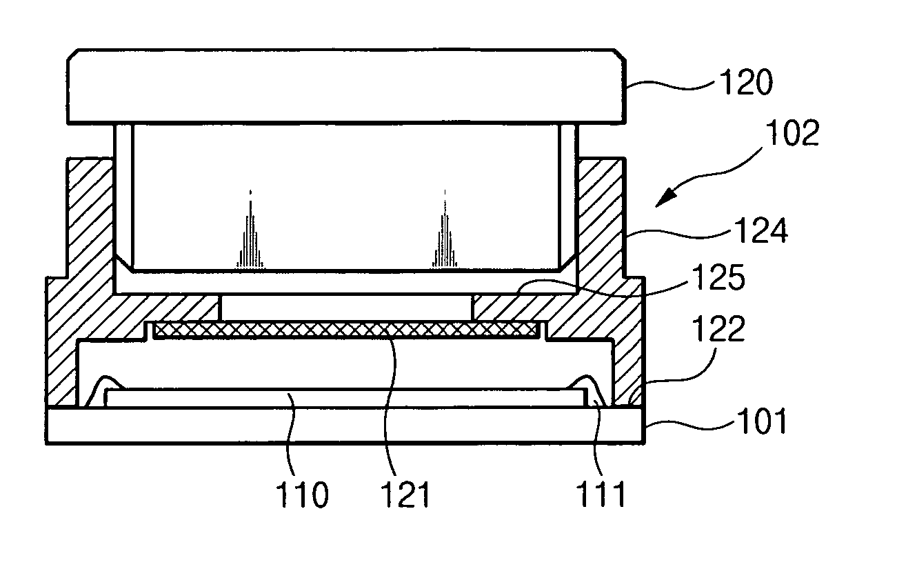
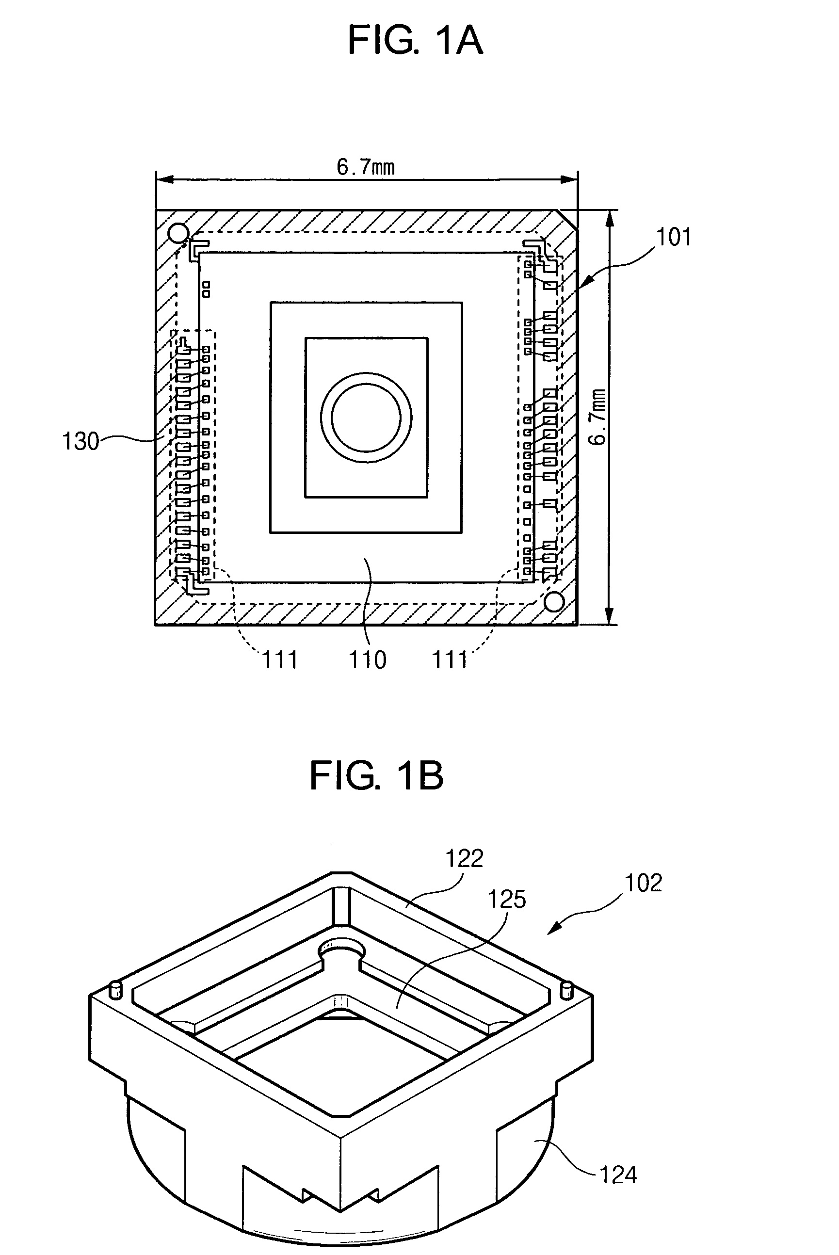
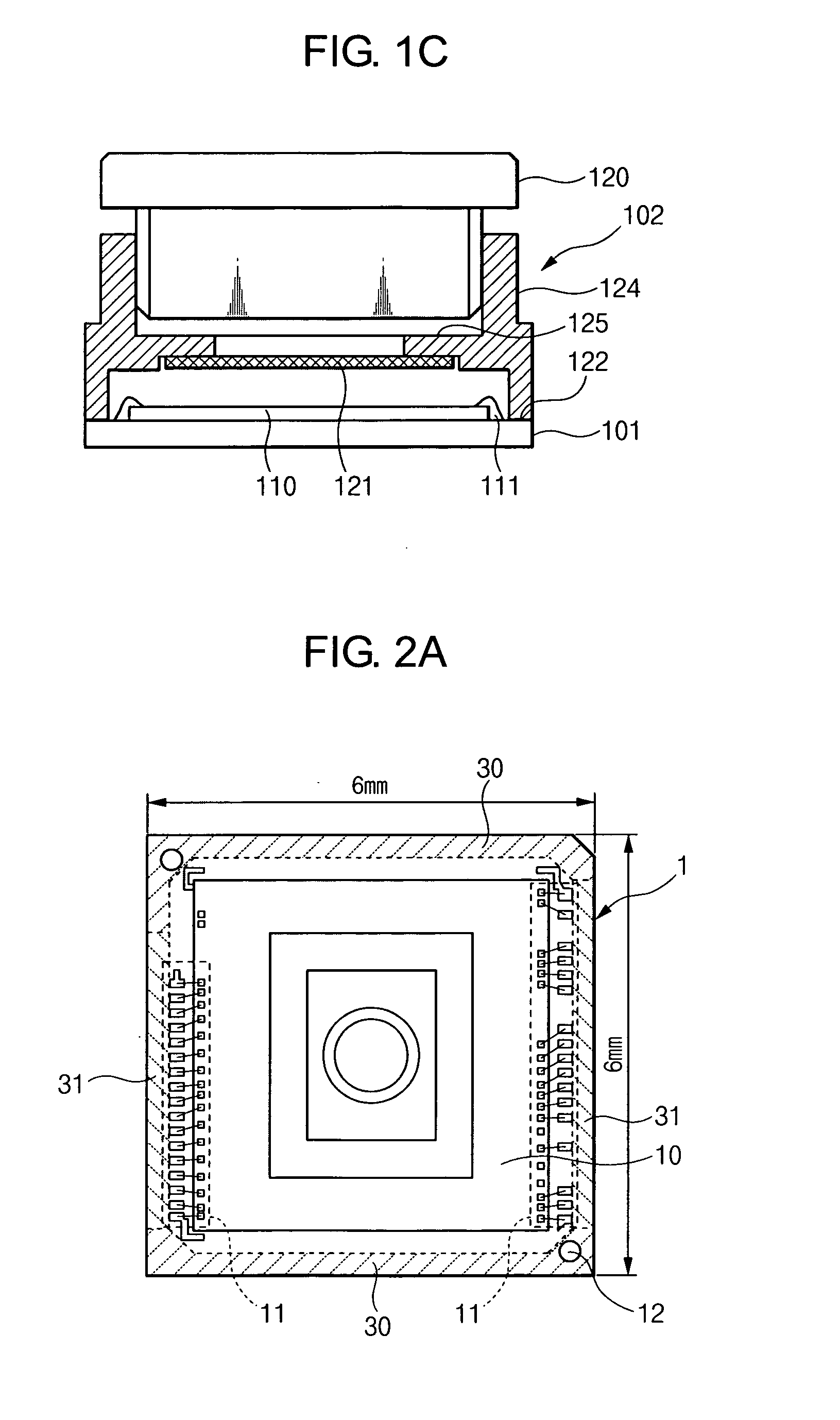
[0077]FIG. 4A is a plan view illustrating the PCB 1 in which an image sensor 10 according to the invention is electrically connected by wire bonding sections 11, and FIG. 4B is a perspective bottom view illustrating a housing 2 which is joined on the PCB 1 of FIG. 4A. Hereinafter, the descriptions overlapped with those of the above-described embodiment will be omitted.
[0078] Referring to FIG. 4A, the image sensor 10 is attached on the PCB 1, the image sensor 10 and the PCB 1 are electrically connected by the wire bonding sections 11, and the wire bonding sections 11 are formed in three directions, that is, in the left, right, and lower sides of the image sensor 10.
[0079] On the edge of the PCB 1, filling regions 31, in which the adhesive 3 is filled, are formed in three directions where the wire bonding sections 11 are present, and a joining region 30 is formed in one direction where the wire bonding section 11 is not present. The joining region 30 is joined to a joining section 22...
second modified embodiment
[0082]FIG. 5A is a plan view illustrating a PCB 1 in which an image sensor 10 according to the invention is electrically connected by wire bonding sections 11, and FIG. 5B is a perspective bottom view illustrating a housing 2 which is joined on the PCB 1 of FIG. 5A. Hereinafter, the descriptions overlapped with those of the above-described embodiment will be omitted.
[0083] Referring to FIG. 5A, the image sensor 10 is attached on the PCB 1, the image sensor 10 and the PCB 1 are electrically connected by the wire bonding sections 11, and the wire boding sections 11 are formed in four directions of the image sensor 10.
[0084] On the edge of the PCB 1, filling regions 31 in which the adhesive 3 is filled are formed in four directions where the wire bonding sections 11 are present, and joining regions 30 are formed in four corners of the PCB 1, that is, in the portions where the wire bonding sections 11 are not present. The joining regions 30 are joined to joining sections 22 (refer to F...
PUM
Abstract
The present invention relates to a camera module, and more particularly, to a camera module which is miniaturized by changing the structure of a housing joined to a PCB on which a standardized image sensor is wire-bonded and a method of manufacturing the camera module. The camera module includes a PCB to which an image sensor is connected by a wire bonding section; and a housing that holds a lens section. The housing includes a joining section that is joined to the side where the wire bonding section of the PCB is not formed; and a step section that is formed to recede in a portion corresponding to the wire bonding section of the PCB.
Description
CROSS-REFERENCE TO RELATED APPLICATIONS [0001] The application claims the benefit of Korea Patent Application No. 2005-0029388 filed with the Korea Industrial Property Office on Apr. 8, 2005, the disclosure of which is incorporated herein by reference. BACKGROUND OF THE INVENTION [0002] 1. Field of the Invention [0003] The present invention relates to a camera module, and more particularly, to a camera module which is miniaturized by changing the structure of a housing joined to a PCB on which a standardized image sensor is wire-bonded and a method of manufacturing the camera module. [0004] 2. Description of the Related Art [0005] In general, a camera module is an imaging device which is used in a video camera, a digital camera, a PC camera, a mobile phone, and a PDA for the recognition of an image. A miniaturized camera module is built in such products. [0006] Recently, as the functions of a mobile phone have become diverse and complex, it is required that parts and devices which a...
Claims
Application Information
Patent Timeline
Application Date:The date an application was filed.
Publication Date:The date a patent or application was officially published.
First Publication Date:The earliest publication date of a patent with the same application number.
Issue Date:Publication date of the patent grant document.
PCT Entry Date:The Entry date of PCT National Phase.
Estimated Expiry Date:The statutory expiry date of a patent right according to the Patent Law, and it is the longest term of protection that the patent right can achieve without the termination of the patent right due to other reasons(Term extension factor has been taken into account ).
Invalid Date:Actual expiry date is based on effective date or publication date of legal transaction data of invalid patent.

