Display device

a display device and liquid crystal technology, applied in non-linear optics, instruments, optics, etc., can solve the problems of frame-like luminance difference generation and disturbance of liquid crystal orientation, and achieve the effect of preventing the generation of frame-like luminance differen

Inactive Publication Date: 2006-11-23
PANASONIC LIQUID CRYSTAL DISPLAY CO LTD +1
View PDF8 Cites 6 Cited by
  • Summary
  • Abstract
  • Description
  • Claims
  • Application Information

AI Technical Summary

Benefits of technology

[0010] The present invention has been made in view of such circumstances, and it is an object of the present invention to provide a liquid crystal display device in which it is possible to prevent the generation of a frame-like luminance difference in a portion which surrounds the light transmissive region.

Problems solved by technology

However, with respect to the liquid crystal display device having such a constitution, it has been found that a frame-like luminance difference is generated at the periphery of the hole formed in the insulation film (light transmissive region) at the time of image display.
As a result of an extensive study of the causes of such a phenomenon, it has been found that, since a steep stepped portion is formed at a portion corresponding to a side wall surface of the hole formed in the insulation film, a disturbance of the orientation of the liquid crystal is liable to be easily generated, whereby, at the time of producing a black display in the light transmissive mode, for example, a complete black display cannot be obtained in such a portion, thus giving rise to the above-mentioned drawback.

Method used


Image

  • Display device
  • Display device
  • Display device

Examples


embodiment 1

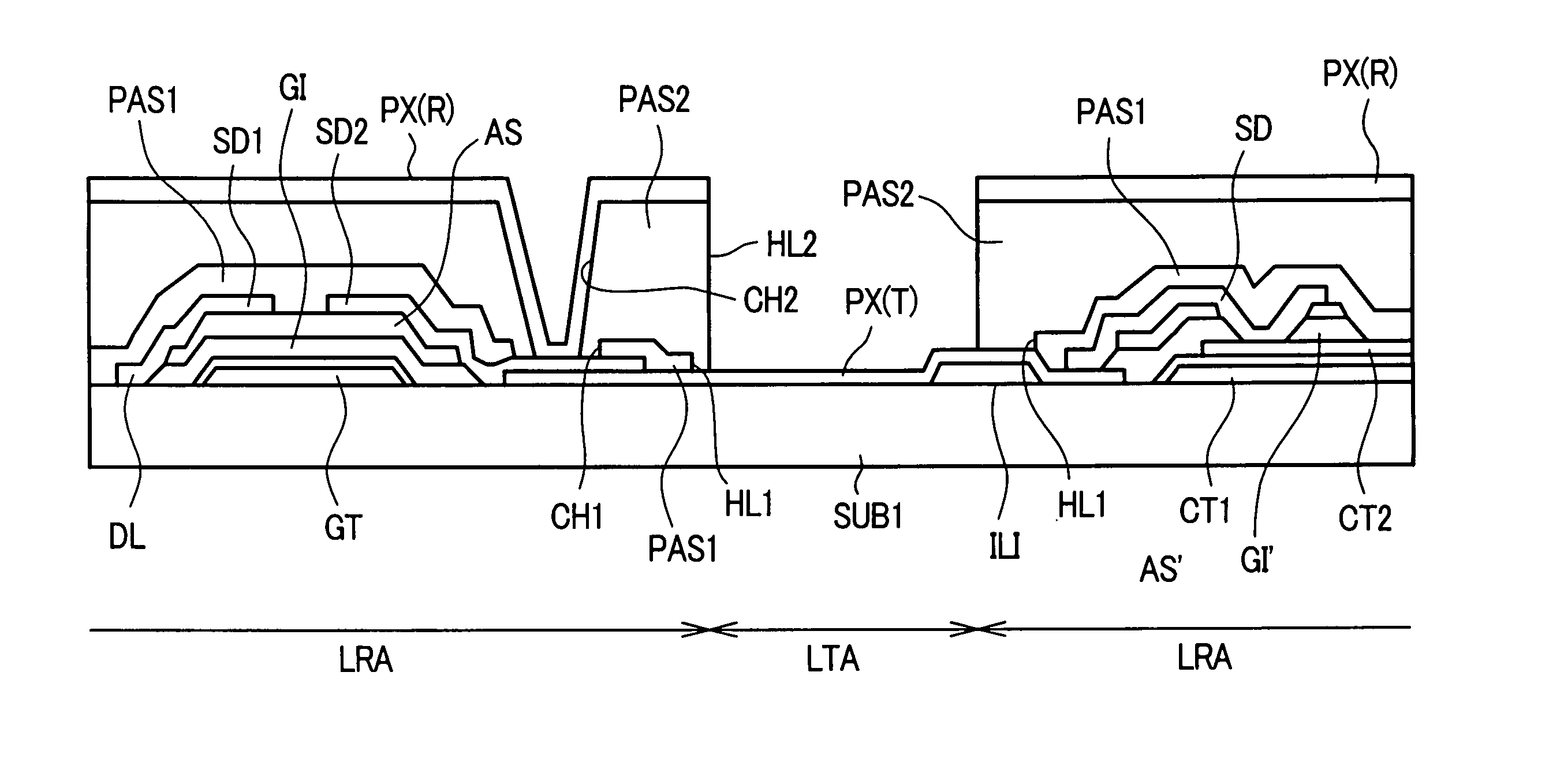
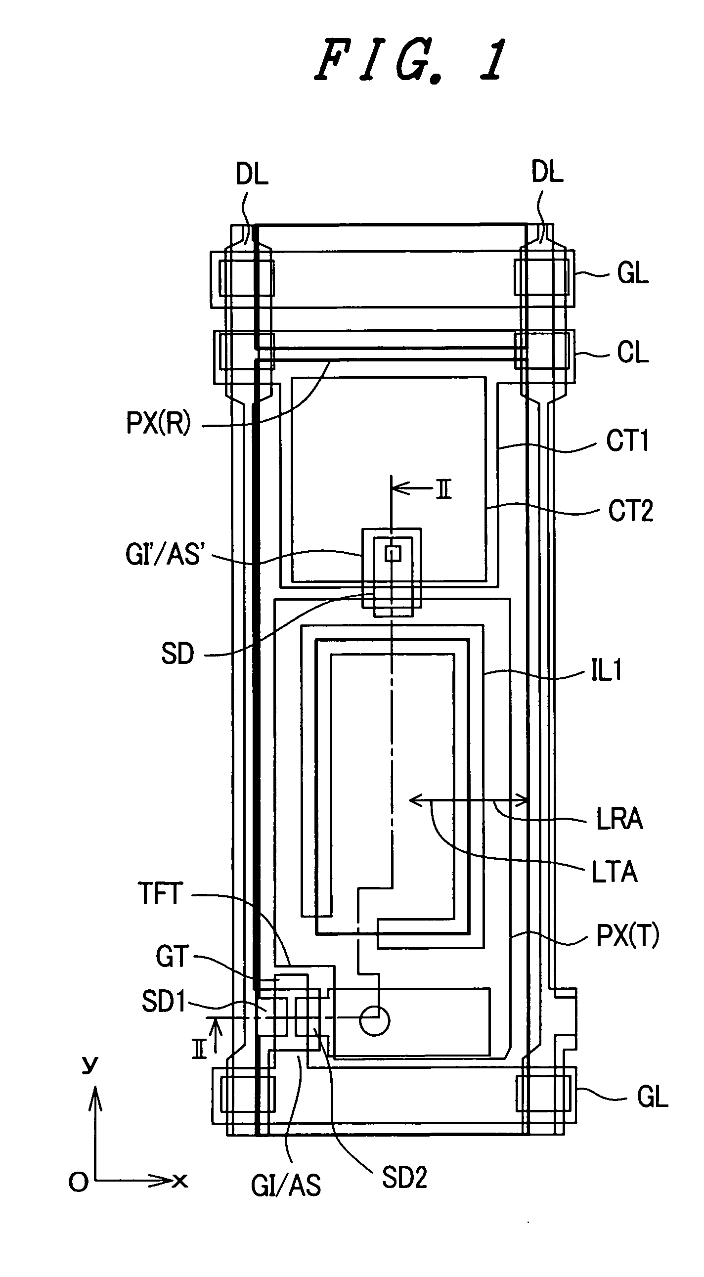
[0028]FIG. 1 is a plan view showing one embodiment of the constitution of a pixel of a liquid crystal display device according to the present invention. Further, FIG. 2 is a cross-sectional view taken along a line II-II in FIG. 1.

[0029] Pixels as seen in these drawings are formed within regions which are defined by gate signal lines GL, which extend in the x direction and are juxtaposed in the y direction, and drain signal lines DL, which extend in the y direction and are juxtaposed in the x direction (pixel regions).

[0030] First, the above-mentioned gate signal lines GL are formed on the liquid-crystal-side surface of the transparent substrate SUB1. The gate signal line GL has a portion which is extended slightly to the pixel region side and this extended portion forms a gate electrode GT of a thin film transistor TFT, as will be explained in more detail later. This gate signal line GL and the gate electrode GT are made of, for example, aluminum (Al) or an alloy thereof and an an...

embodiment 2

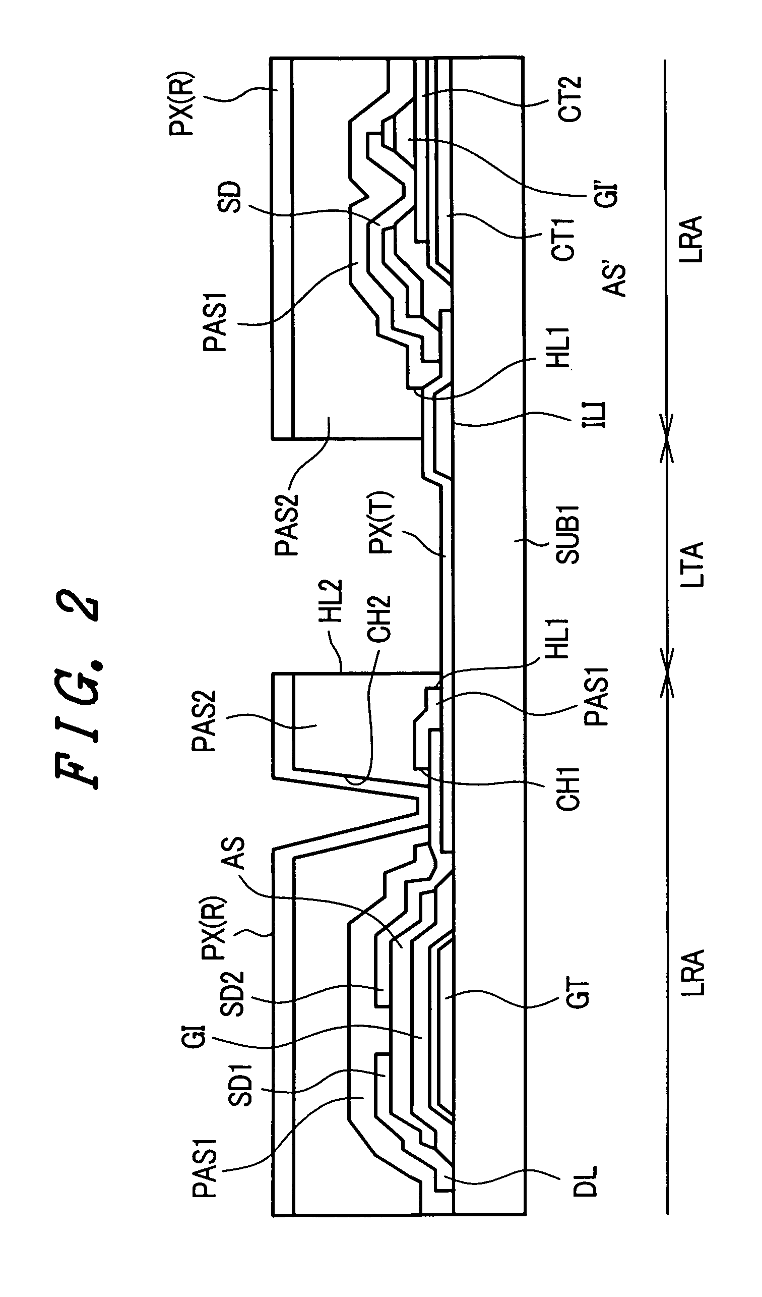
[0063]FIG. 4 is a plan view showing another embodiment of the pixel of the liquid crystal display device according to the present invention, similar tot hat of FIG. 1.

[0064] The constitution which makes this embodiment different from the embodiment shown in FIG. 1 lies in the fact that the light shielding layer ILI is formed not only in the vicinity of the thin film transistor TFT within the boundary portion between the light transmissive region LTA and the light reflective region LRA, but also in other portions within such a boundary portion, for example, in the vicinity of the capacitive element Cstg.

[0065] This constitution is provided for eliminating, with high probability, the drawback that occurs when the pixel electrode PX (T) is formed by extending it over the light shielding layer ILI, such that it is broken at the stepped portion of the light shielding layer ILI.

embodiment 3

[0066]FIG. 5 is a plan view showing another embodiment of a pixel of the liquid crystal display device according to the present invention and it shows an arrangement similar to that of FIG. 1.

[0067] The constitution which makes this embodiment different from the embodiment shown in FIG. 1 lies in the fact that the light shielding layer ILI is formed continuously along the whole area of the boundary portion between the light transmissive region LTA and the light reflective region LRA.

[0068] This embodiment is based on the understanding that, if the drawback which is generated when the pixel electrode PX (T) is formed to extend over the light shielding layer ILI can be eliminated by any means, it is unnecessary for the boundary portion between the light transmissive region LTA and the light reflective region LRA to have a portion where the light shielding layer is not formed along that boundary.

[0069] Here, as the means for eliminating such a drawback, for example, by forming the l...


PUM

PropertyMeasurementUnit
luminanceaaaaaaaaaa
transparentaaaaaaaaaa
light transmissive conductiveaaaaaaaaaa

Abstract

The present invention prevents a frame-like luminance difference generated in a portion which surrounds a light transmissive region. In a pixel region formed on a substrate, a first pixel electrode formed of a light transmissive conductive layer is formed in one light transmissive region which is formed by partitioning the pixel region and a second pixel electrode formed of a non-light transmissive conductive film is formed on the other light reflective region. The first pixel electrode is positioned as a lower layer with respect to an insulation film. A hole is formed in the insulation film in a region corresponding to the light transmissive region so as to expose the first pixel electrode. The second pixel electrode is formed on a light reflective region of the insulation film. Light shielding is performed at a portion corresponding to a side wall surface of the hole formed in the insulation film.

Description

CROSS REFERENCE TO RELATED APPLICATION [0001] This application is a divisional application of U.S. application Ser. No. 10 / 629,631, filed Jul. 30, 2003, the contents of which are incorporated herein by reference.BACKGROUND OF THE INVENTION [0002] The present invention relates to a liquid crystal display device, and, more particularly, to a liquid crystal display device of the partial transmissive type, in which it is possible to eliminate a frame-like luminance difference around the periphery of the light transmissive region in each pixel. [0003] A liquid crystal display device of the partial transmissive type is used as a miniaturized liquid crystal display device for a mobile telephone or the like. This liquid crystal display device allows a user to recognize images on a display screen using light made up of the reflective light of the sun (a light reflection mode) or using light from a backlight incorporated in the liquid crystal display device (a light transmissive mode), depend...

Claims


Application Information

Patent Timeline
Patent Type & Authority Applications(United States)
IPC IPC(8): G02F1/136G02F1/1335G02F1/1333G02F1/1343G02F1/1368
CPCG02F1/133371G02F1/133512G02F2203/09
Inventor ANNO, KOUICHIKOMENO, HITOSHINISHINO, TOMONORI
Owner PANASONIC LIQUID CRYSTAL DISPLAY CO LTD
Why Eureka
Try Eureka