Display device

a technology of display device and bezel, which is applied in the direction of semiconductor devices, instruments, electrical devices, etc., can solve the problems of large bezel and complicated design of such devices, and achieve the effects of reducing the bezel of the device, preventing the appearance of luminance differences, and reducing the luminance differen

Active Publication Date: 2021-08-05
SAMSUNG DISPLAY CO LTD
View PDF0 Cites 1 Cited by
  • Summary
  • Abstract
  • Description
  • Claims
  • Application Information

AI Technical Summary

Benefits of technology

[0028]According to the embodiments, it is possible to prevent a luminance difference from occurring, or to reduce a difference in luminance that occurs, at an edge of a display device and to reduce a bezel thereof.

Problems solved by technology

In addition, in order to drive each pixel of the organic light emitting diode display more efficiently, a design thereof becomes more complicated, and as the number of wires to supply a voltage to drive the pixel increases, a bezel becomes large.

Method used


Image

  • Display device
  • Display device
  • Display device

Examples


Embodiment Construction

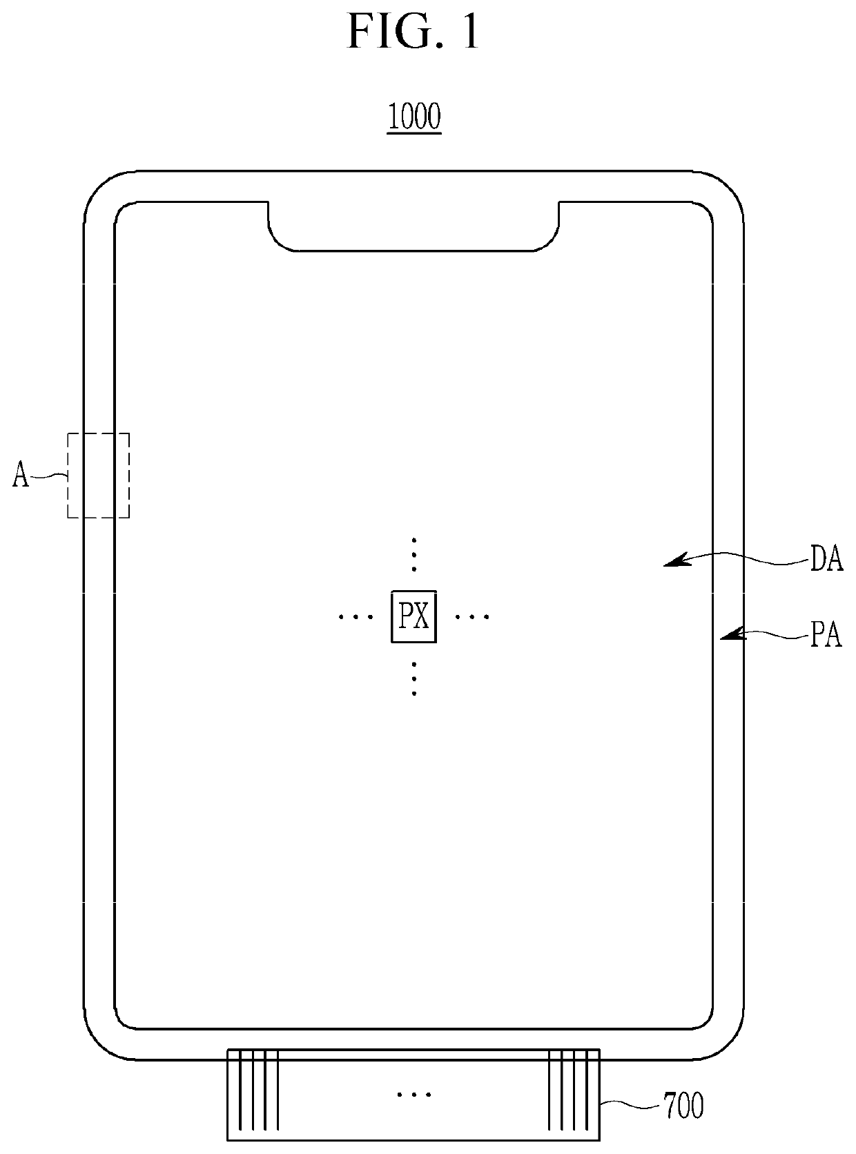
[0046]The present disclosure will be described more fully hereinafter with reference to the accompanying drawings, in which exemplary embodiments of the present disclosure are shown. As those of ordinary skill in the art would realize, the described embodiments may be modified in various and suitable different ways, all without departing from the spirit or scope of the present disclosure.

[0047]Parts (e.g., elements and / or features) that are irrelevant to the description may be omitted to clearly describe the present disclosure, and like reference numerals designate like elements throughout the specification.

[0048]Further, in the drawings, the size and thickness of each element may be exaggerated for ease of description, and the present disclosure is not limited by the embodiments illustrated in the drawings. In the drawings, the thicknesses of layers, films, panels, areas, regions, etc., may be exaggerated for clarity. In the drawings, for ease of description, the thicknesses of som...


PUM

PropertyMeasurementUnit
constant voltageaaaaaaaaaa
areaaaaaaaaaaa
reference voltageaaaaaaaaaa

Abstract

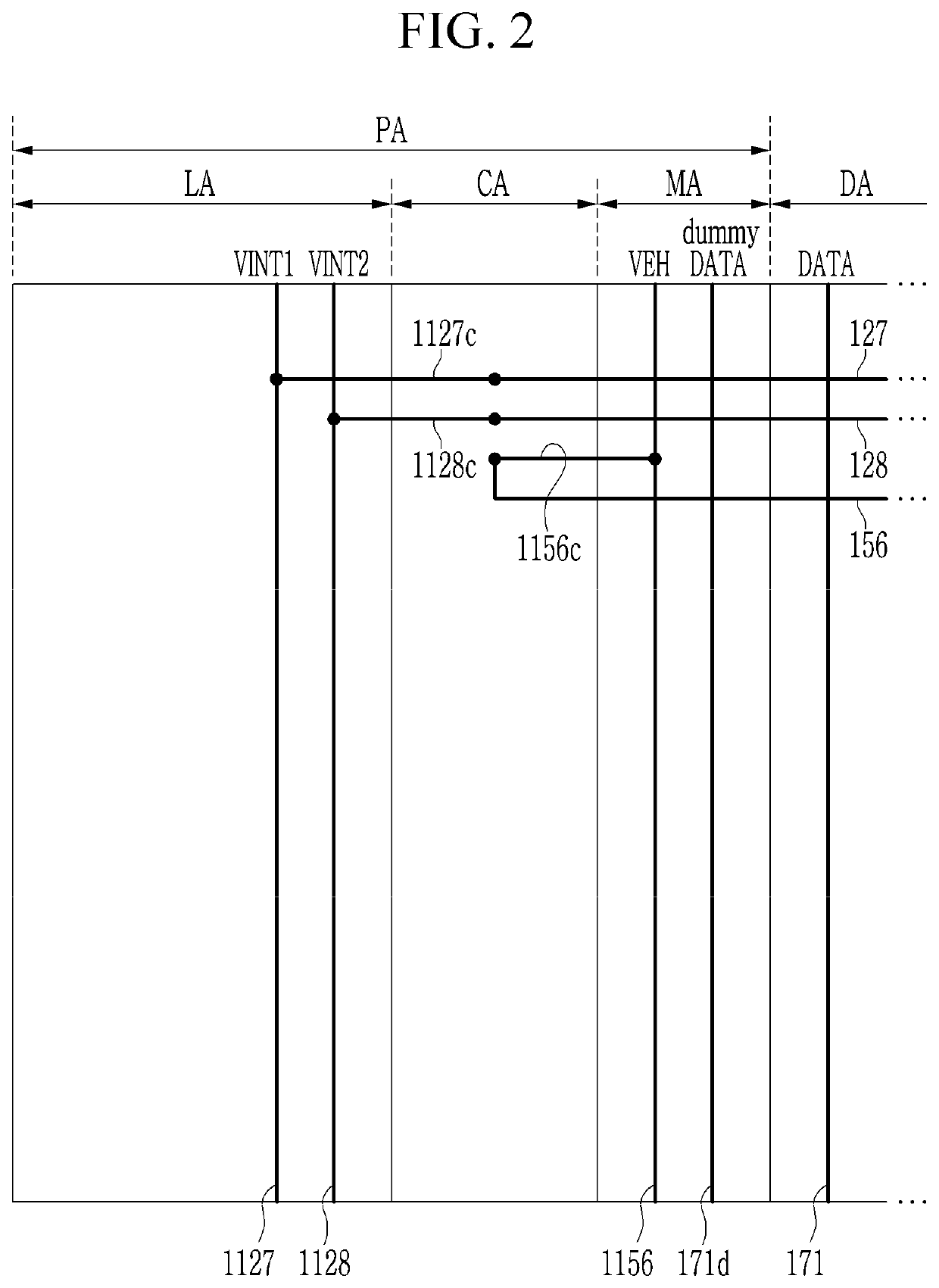
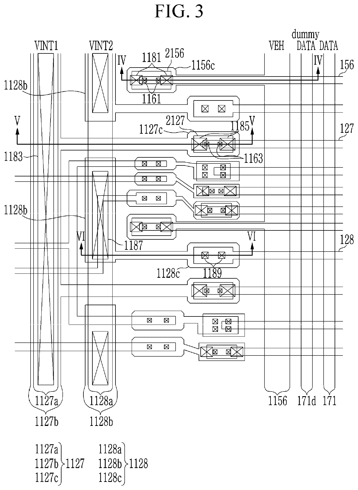
An embodiment provides a display device including: a display area including a plurality of pixels; a dummy area adjacent to an edge of the display area; a reference voltage supplying line in the dummy area and to supply a reference voltage; and a wire area in which a wire to supply a signal applied to the display area is located, wherein a pixel of the plurality of pixels includes a light emitting diode coupled between a driving voltage line to which a driving voltage is to be applied and a common voltage line to which a common voltage is to be applied, and a driving transistor coupled between the driving voltage line and the light emitting diode, and wherein the reference voltage is to be supplied to a first electrode of the driving transistor.

Description

CROSS-REFERENCE TO RELATED APPLICATION[0001]This application claims priority to and the benefit of Korean Patent Application No. 10-2020-0011184, filed on Jan. 30, 2020, the entire content of which is hereby incorporated by reference.BACKGROUND1. Field[0002]Embodiments of the present disclosure relates to a display device.2. Description of the Related Art[0003]An organic light emitting diode (OLED) display device includes two electrodes and an organic light emitting layer interposed therebetween, wherein electrons injected from one electrode and holes injected from another electrode are combined in the organic light emitting layer to generate excitons. The generated excitons are changed (e.g., transition) to a ground state from an excited state, releasing energy to emit light.[0004]Each pixel of the organic light emitting diode display may be coupled to a data line, a driving voltage line, or the like to receive a voltage. When one data line and one driving voltage line are coupled ...

Claims


Application Information

Patent Timeline
Patent Type & Authority Applications(United States)
IPC IPC(8): G09G3/3258G09G3/3291H01L27/32
CPCG09G3/3258G09G2300/0413H01L27/3276G09G3/3291G09G2300/0426G09G2300/0819G09G2300/0842G09G2300/0861G09G2310/0251G09G2310/0262G09G3/3233H10K59/131G09G3/3208G09G2310/0245G09G2300/0809G09G2300/0439H10K59/88H10K59/1213H10K50/80
Inventor CHO, YOUNG JINSEO, MYEONG HEEKIM, YANG WAN
Owner SAMSUNG DISPLAY CO LTD
Why Eureka
Try Eureka