Image sensor with shared voltage converter for global shutter operation

a technology of image sensor and global shutter operation, applied in the field of image sensors, can solve the problems of high power consumption, noise from signal transfer to various nodes, lack of uniform conversion of accumulated charge to voltage, etc., and achieve the effect of maximizing the area of photo-diodes and the fill factor of pixels

Inactive Publication Date: 2007-01-18
SAMSUNG ELECTRONICS CO LTD
View PDF13 Cites 90 Cited by
  • Summary
  • Abstract
  • Description
  • Claims
  • Application Information

AI Technical Summary

Benefits of technology

[0020] The present invention may be used to particular advantage when the image sensor is a CMOS (complementary metal oxide semiconductor) image sensor. However, the present invention may also be used for other types of image sensors.
[0021] In this manner, the voltage converter is shared among the plurality of pixels for minimizing the area occ

Problems solved by technology

However, the CCD-type image sensor continuously transfers charge carriers undesirably resulting in high power consumption.
However in the CMOS image sensor, as the accumulated charge is converted into a signal voltage in each pixel, noise may arise from transfer of signals to various nodes.
In addition, the pixels of the CMOS image sensor each have a respective voltage conversion circuit

Method used


Image

  • Image sensor with shared voltage converter for global shutter operation
  • Image sensor with shared voltage converter for global shutter operation
  • Image sensor with shared voltage converter for global shutter operation

Examples


Embodiment Construction

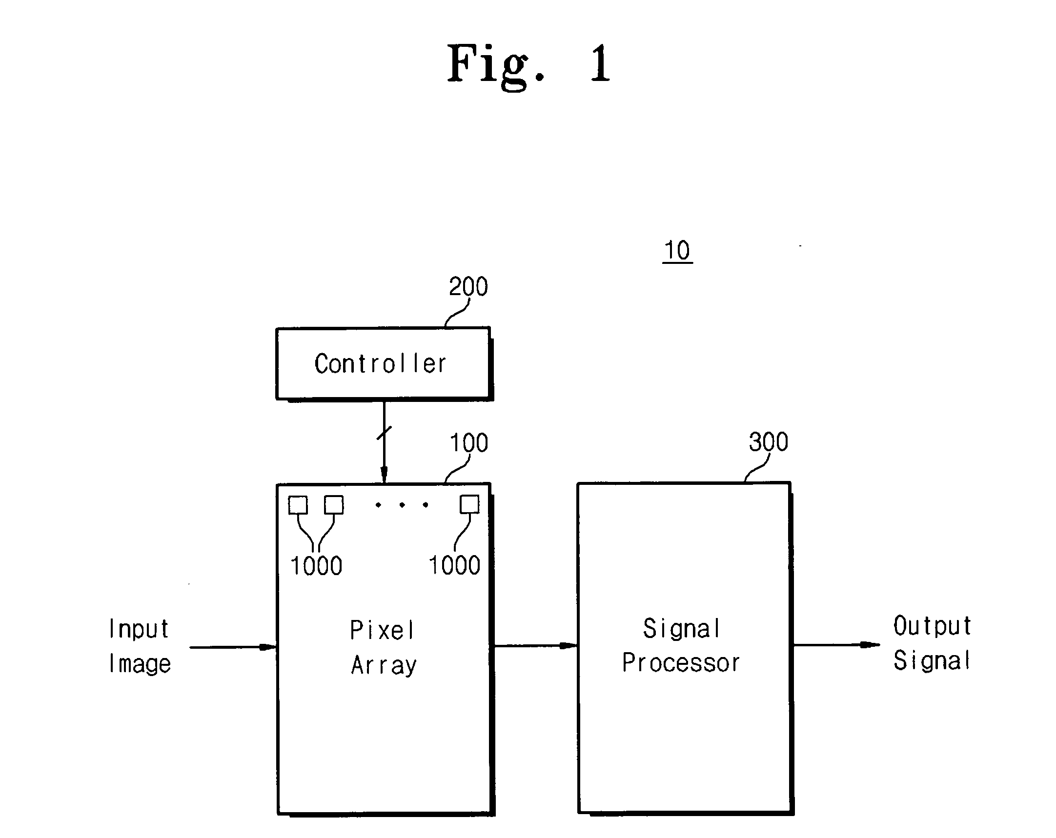
[0031]FIG. 1 is a block diagram of a CMOS (complementary metal oxide semiconductor) image sensor in accordance with a preferred embodiment of the present invention. The CMOS image sensor 10 includes a pixel array 100, a controller 200, and a signal processor 300. The pixel array 100 includes rows and columns of pixels for converting an image into electrical signals. Each pixel photo-converts light of the image to generate a respective voltage at a respective location of the array.

[0032] The controller 200 generates control signals for driving the pixels of the pixel array 100. The signal processor 300 converts the respective voltages from the pixels of the pixel array 100 including converting an analog voltage into a digital signal with removal of noise.

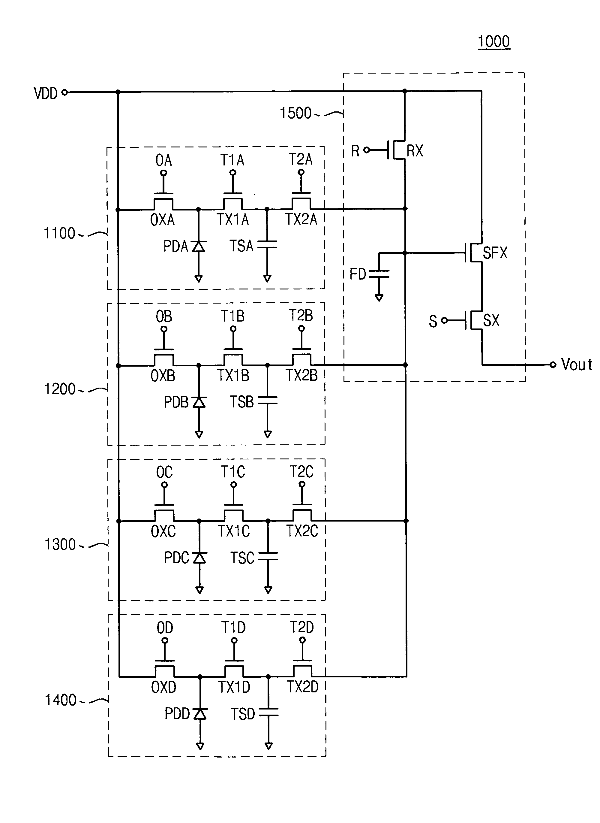
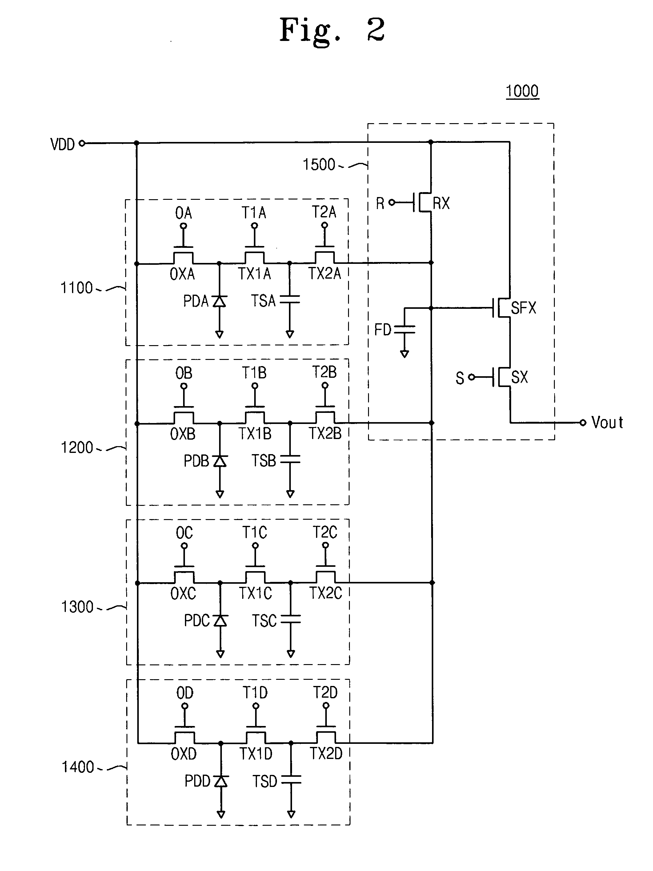
[0033] In one embodiment of the present invention, the pixel array 100 is comprised of an array of active pixel sensor (APS) units 1000, each having multiple pixels sharing a voltage converter.

[0034]FIG. 2 shows a circuit diagram ...


PUM


Abstract

Each of a plurality of pixels includes a respective photo-converting unit and a respective charge storing unit. The respective photo-converting unit generates respective charge from an image, and the respective charge storing unit stores the respective charge. The respective charges are generated and stored simultaneously, and converted into respective voltages sequentially by a shared voltage converter.

Description

BACKGROUND OF THE INVENTION [0001] This application claims priority to Korean Patent Application No. 2005-64417, filed on Jul. 15, 2005 in the Korean Intellectual Property Office, the disclosure of which is incorporated herein in its entirety by reference. [0002] 1. Field of the Invention [0003] The present invention relates generally to image sensors, and more particularly to using a shared voltage converter for performing a global shutter operation among a plurality of pixels. [0004] 2. Description of the Related Art [0005] Image sensors that convert images into electrical signals are generally classified into one of a charge-coupled device (CCD) type or a complementary metal-oxide-semiconductor (CMOS) type depending on accumulation of electrons or holes and on the mechanism of charge transfer. The CMOS image sensor is also referred to as a CIS. [0006] The CCD-type image sensor transfers accumulated electrons toward an output port using gate pulses for charge coupling and then con...

Claims


Application Information

Patent Timeline
IPC IPC(8): H04N5/335
CPCH04N5/335H04N25/00H04N25/60H04N25/77
Inventor AHN, JUNG-CHAKLEE, YONG-HEEPARK, JONG-EUN
Owner SAMSUNG ELECTRONICS CO LTD
Why Eureka
Try Eureka