Optical system and method for improving imaging properties thereof

an optical system and imaging technology, applied in the field of optical systems, can solve the problems of insufficient deterministic optimization methods, inaccurate approach, and ineffective correction of image defects, so as to reduce the number of discarded optical components, reduce the manufacturing cost of the optical system, and improve the effect of image quality

Inactive Publication Date: 2007-03-29
CARL ZEISS SMT GMBH
View PDF23 Cites 3 Cited by
  • Summary
  • Abstract
  • Description
  • Claims
  • Application Information

AI Technical Summary

Benefits of technology

[0019] The new approach makes it possible to effectively correct image defects which are not substantially affected by the assembly of the optical elements into the entire optical system. Other image defects, which result from the assembly of the entire optical system, for example image defects induced by mechanical stress exerted by mounts of optical components or caused by manufacturing tolerances, can be corrected by the subsequent optimization method involving the in situ measuring of image defects of movable parts.
[0020] Another advantage of the new approach is the ability to employ optical components in the manufacture of the optical system that individually would not meet the tight specifications that prevail in sophisticated optical systems, e.g. projection objectives used in microlithographic exposure apparatus. In a conventional approach, manufacturing tolerances, for example tolerances relating to the surface shape of the optical component, are calculated for each optical component on the basis of the overall specification of the optical system. An optical component that does not meet the specification calculated specifically for this component is usually discarded. According to the new approach, however, there is a substantial probability that such an optical component may nevertheless be used in the assembly of the optical system. This is due to the fact that optical defects caused by the inferior optical component may be substantially corrected for by the other optical components of the optical element if these are assembled in their optimum target positions calculated in the pre-optimization process. This decreases the number of discarded optical components and therefore substantially reduces the manufacturing costs of the optical system.
[0021] In an advantageous embodiment the manufacture of the optical components is not finished before they are measured during the pre-optimization process. If it is discovered that an optical component has to be discarded because otherwise the overall image defect of the optical element exceeds a predetermined threshold value, this is cheaper than discarding an optical component that is ready for being installed in the optical system. For example, if the optical components are lenses made of lens blanks, it is advantageous to individually measure a deviation from a specification relating, e.g., to the inhomogeneity of the refractive index or the birefringence tensor, of one or more lens blanks instead of measuring this quantity of the grinded, polished and coated lenses. Substantial cost savings are achieved if a lens blank has to be discarded instead of a grinded, polished and coated lens.
[0022] According to a second aspect of the invention, the optical system comprises a correcting optical element for correcting an image defect. The correcting optical element has at least two distinct configurations. Computing means are provided for representing the optical effect of the correcting optical element in the at least two distinct configurations as linear combinations of base functions of an orthogonal function set. When calculating a target position for the at least two optical elements, the effect of the correcting optical elements is integrally considered as a free parameter, and thus an optimum configuration of the correcting optical element is determined so as to further reduce the overall image defect.

Problems solved by technology

Since many image defects are produced only during assembly, for example as a result of stress induced by lens mounts, such an approach has proven to be too inaccurate.
Such optimization methods are insufficiently deterministic.
This procedure is too tedious and complicated since the number of possible positions is very large, and therefore measurements are extremely time consuming.
In the same way as when finding the most favorable rotational position, here too the experience of the respective technician was decisive in finding useful degrees of freedom, which however led to adjustment results that were not deterministically reproducible.
Often the choice of the lenses to be moved as well as the choice of the degrees of freedom of movement were very time-consuming and also did not always achieve given specifications.
But also in these cases a multidimensional problem exists if several lenses within a projection objective lens system can be moved.
As a result an optimal position configuration of all movable lenses in which the overall image defect usually falls below given specifications, or an absolute minimum cannot be found with reasonable effort and expenditure.
For example, it is difficult with this known method to correct image defects having a higher azimutal order.
Such image defects may be caused by lenses or other optical components having significant inhomogeneities of the refractive index and / or non-rotationally symmetric surface defects.

Method used


Image

  • Optical system and method for improving imaging properties thereof
  • Optical system and method for improving imaging properties thereof
  • Optical system and method for improving imaging properties thereof

Examples


first embodiment

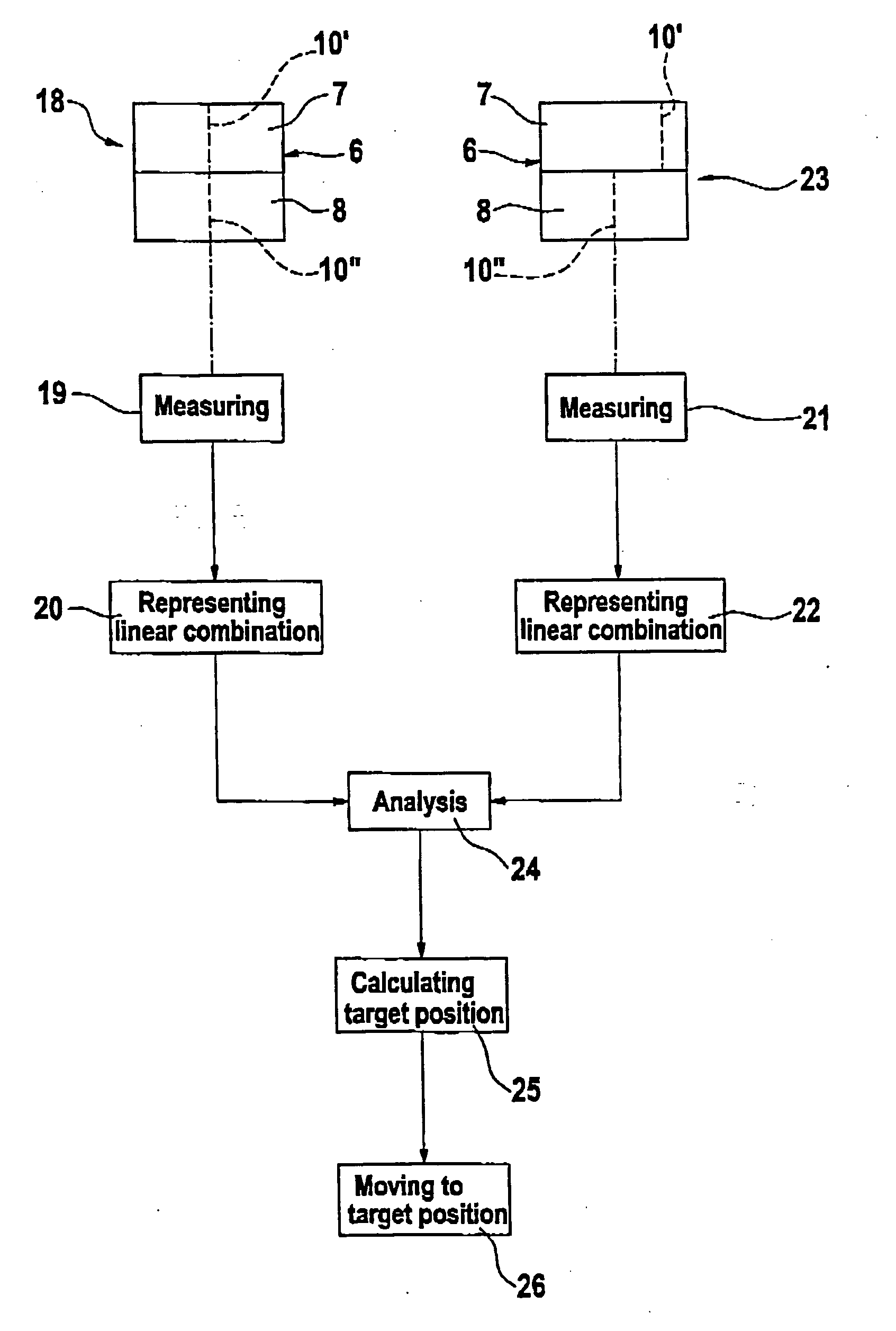
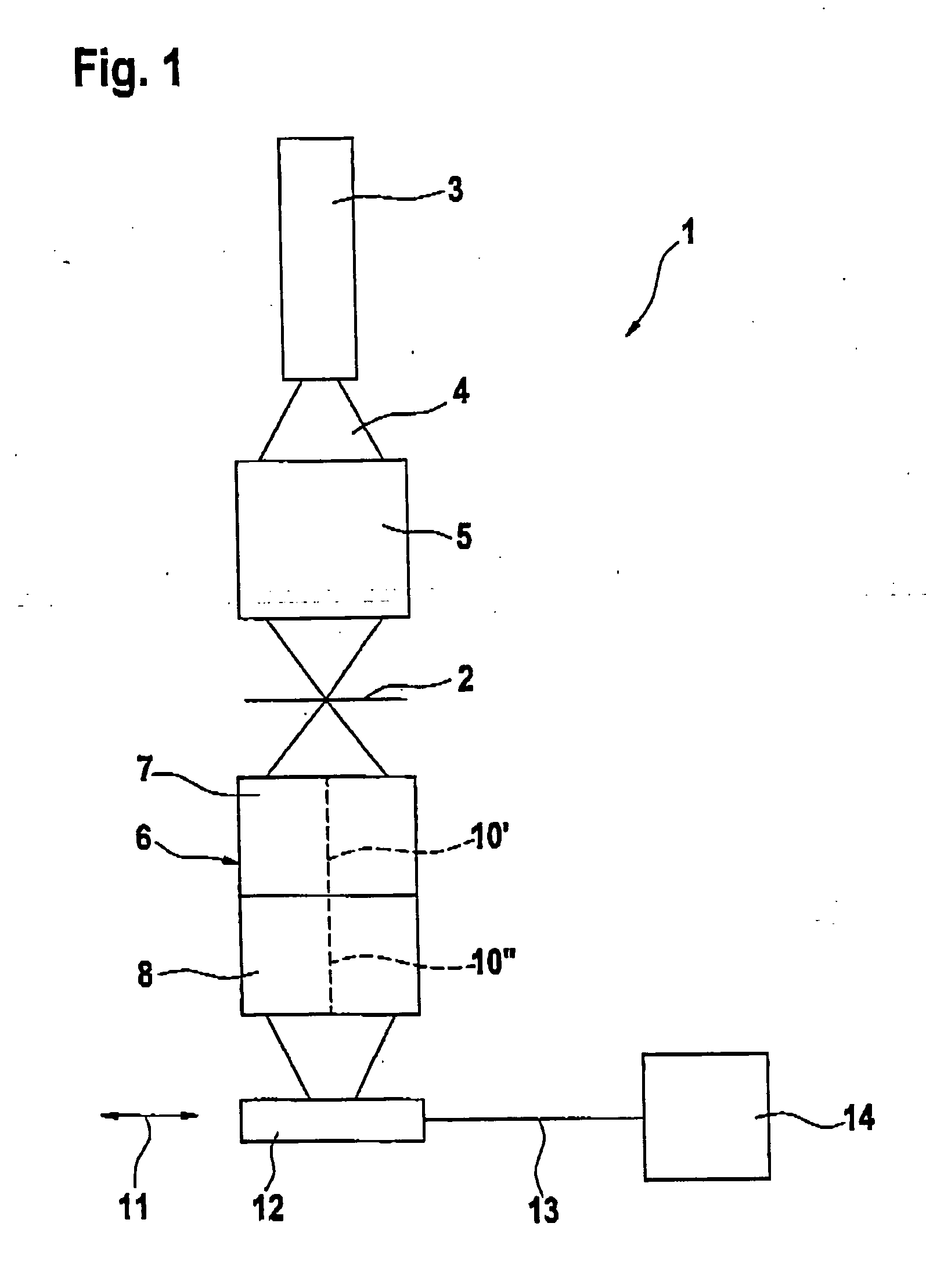
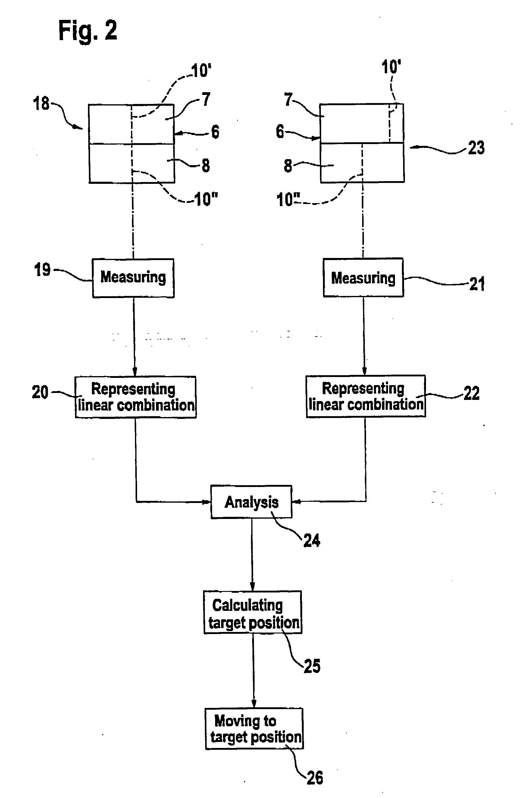
[0121] The method steps in addition to those shown in FIG. 4 are carried out, after a subdivision of the projection objective 406 in optical elements 430 to 433 has been established. The pre-optimization is then carried out for all optical elements 430 to 433.

second embodiment

[0122] A second embodiment for such a preoptimization will be further described in more detail with reference to the flow diagram shown in FIG. 9:

[0123] According to this second embodiment, the additional method steps are introduced between an initializing step 440 and the measuring step 441. In the initializing step 440 the projection objective 406 is divided into a movable part suitable for the later measurement step 441 and a stationary part, as has been explained further above. The steps to be carried out in the pre-optimization procedure between the initializing step 440 and the measurement step 441 are, at least in principle, identical for both embodiments and are for that reason described hereinafter for both embodiments.

[0124] Referring to FIG. 8, the projection objective 406 may be divided in the initializing step 440 into a first part, which can be moved in its entirety and consists of the optical element 430, and a second stationary part comprising the optical elements 4...


PUM


Abstract

An optical system has at least two optical elements whose spatial relation with respect to each other can be changed. At least one of the optical elements comprises a plurality of optical components. The optical system comprises first measuring means for individually measuring an image defect of each optical component, and first computing means for computing first target positions for the plurality of optical components such that an overall image defect of the at least one of the optical elements is below a predetermined threshold value. Second measuring means are provided for measuring an overall image defect of the optical system, and second computing means represent the measured overall image defect as a linear combination of base functions of an orthogonal function set. The second computing means calculate second target position for the at least two optical elements so as to reduce the overall image defect.

Description

BACKGROUND OF THE INVENTION [0001] 1. Field of the Invention [0002] The present invention relates to an optical system, in particular to a projection objective of a microlithographic projection exposure apparatus, and a method for improving imaging properties of such an optical system. [0003] 2. Description of Related Art [0004] Optical assemblies comprising at least one movable optical element are known on the market, and include projection objectives for microlithographic projection exposure apparatus. With these and other sophisticated optical systems a high image quality is required in order to produce a picture of a structure that is as free of image defects as possible. The movability of at least one optical element within such a projection objective lens system serves to vary the imaging properties of the projection objective lens system with the aim of reducing occurring image defects. [0005] The choice of the position to which a moveable optical element should be adjusted f...

Claims


Application Information

Patent Timeline
Patent Type & Authority Applications(United States)
IPC IPC(8): G06K9/00
CPCG03F7/70258G03F7/706G03F7/705
Inventor STAMMLER, THOMASWAGNER, CHRISTIANREISINGER, GERD
Owner CARL ZEISS SMT GMBH
Why Eureka
Try Eureka