Method of fabricating epitaxial structures

a technology of epitaxial structures and substrates, applied in the direction of sustainable manufacturing/processing, final product manufacturing, led's, etc., can solve the problems of difficult processing and handling of individual cells so formed, poor and inconsistent performance, and high cost of fabricating epitaxial structures. , to achieve the effect of simple and direct removal of substrates, and reduced substrate requirements

Active Publication Date: 2013-06-04
JPMORGAN CHASE BANK NA +1
View PDF14 Cites 551 Cited by
  • Summary
  • Abstract
  • Description
  • Claims
  • Application Information

AI Technical Summary

Benefits of technology

[0003]In accordance with various aspects of the subject invention in at least one embodiment the invention presents an improved method of fabricating epitaxial structures which reduces the number of substrates required for the fabrication process by a factor of two and which admits of a simple and direct removal of the substrate, and the use of a number of different carriers including metals, which does not require singulation before separation from the substrate, and is compatible with further processing.

Problems solved by technology

Fabricating epitaxial structures such as solar cells, LED's, lasers and IR cells is costly and complex.
This process is slow and difficult and can result in poor and inconsistent performance.
The individual cells are then lifted off the substrate by etching along the singulation lines and underneath the individual cells This process is not optimal for mounting onto metal carriers and the individual cells so formed are difficult to process and handle.
Often another material such as epoxy is incorporated, and further processing as well as final cell performance may be limited.
Another shortcoming of such processing is that the wafers or substrates on which the epitaxial layers are grown, is often damaged or rendered unable to be reused, eliminating the cost benefits of epitaxial removal and substrate reuse.

Method used


Image

  • Method of fabricating epitaxial structures
  • Method of fabricating epitaxial structures
  • Method of fabricating epitaxial structures

Examples


Embodiment Construction

[0014]Aside from the preferred embodiment or embodiments disclosed below, this invention is capable of other embodiments and of being practiced or being carried out in various ways. Thus, it is to be understood that the invention is not limited in its application to the details of construction and the arrangements of components set forth in the following description or illustrated in the drawings. If only one embodiment is described herein, the claims hereof are not to be limited to that embodiment. Moreover, the claims hereof are not to be read restrictively unless there is clear and convincing evidence manifesting a certain exclusion, restriction, or disclaimer.

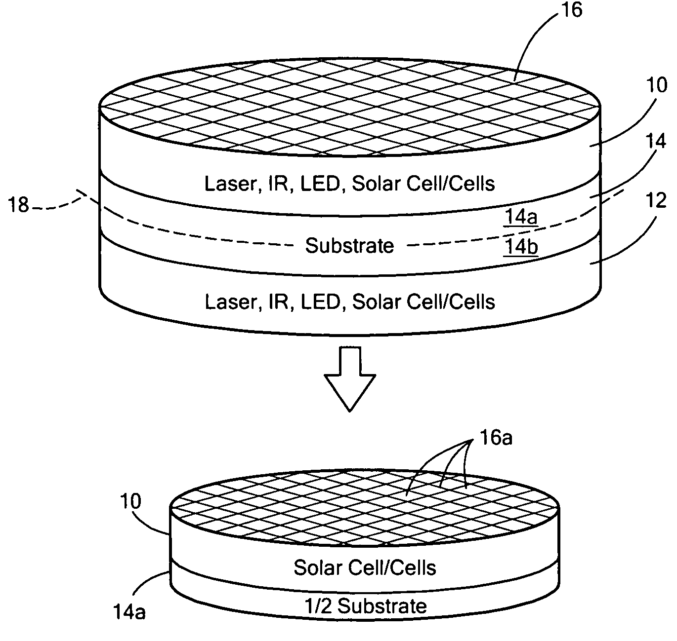
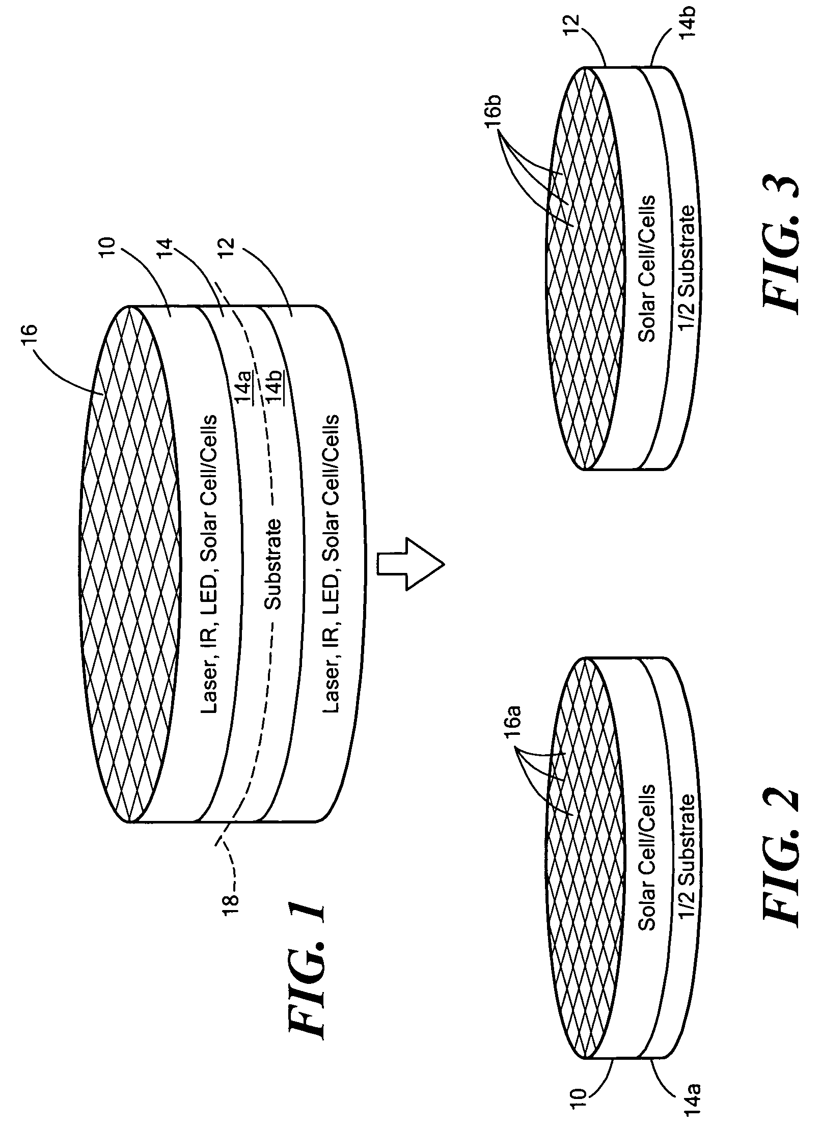
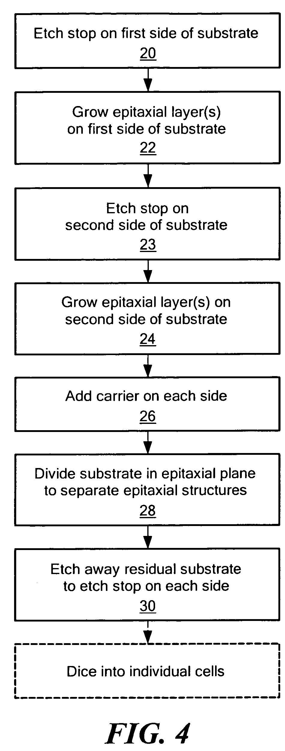
[0015]The method of fabricating epitaxial structures according to this invention in one embodiment employs bi-facial epitaxial growth where both the bottom and the top of the semiconductor wafer or substrate is processed into separate epitaxial structures. The notion is to grow epistructures on one side of the wafer or subs...


PUM


Abstract

A method of fabricating epitaxial structures including applying an etch stop to one side of a substrate and then growing at least one epitaxial layer on a first side of said substrate, flipping the substrate, growing a second etch stop and at least one epitaxial layer on a second side of the substrate, applying a carrier medium to the ultimate epitaxial layer on each side, dividing the substrate into two parts generally along an epitaxial plane to create separate epitaxial structures, removing any residual substrate and removing the etch stop.

Description

FIELD OF THE INVENTION[0001]This invention relates to a method of fabricating epitaxial devices.BACKGROUND OF THE INVENTION[0002]Fabricating epitaxial structures such as solar cells, LED's, lasers and IR cells is costly and complex. Solar cells have been fabricated forming inverted metamorphic (IMM) cells, by depositing the layers such as InGaP, GaAs, and InGaAs on a wafer or substrate such as GaAs often resulting in an array of a multiplicity of solar cells and then applying a carrier and removing the substrate by side etching it away. This process is slow and difficult and can result in poor and inconsistent performance. After removal of the substrate the processed epitaxial layers may be sawed into the individual solar cells. Solar cells have also been made by singulating the multiplicity of cells on, for example, a four inch wafer and then applying a carrier. The individual cells are then lifted off the substrate by etching along the singulation lines and underneath the individu...

Claims


Application Information

Patent Timeline
Patent Type & Authority Patents(United States)
IPC IPC(8): H01L31/18
CPCH01L31/06875H01L31/184H01L31/1892H01L31/0248H01L31/1876H01L33/005H01L33/02H01S5/0202H01L21/02395H01L21/02461H01L21/02463H01L21/02543H01L21/02546Y02E10/544Y02P70/50
Inventor SISKAVICH, BRAD M.
Owner JPMORGAN CHASE BANK NA
Why Eureka
Try Eureka