Electron emission display device
a technology of electron emission display and display device, which is applied in the manufacture of electrode systems, electric discharge tubes/lamps, and discharge tubes luminescnet screens, etc., can solve the problems of deteriorating the screen display quality of electron emission displays, affecting the efficiency of unable to obtain desired white color images at the relevant pixel, etc., to achieve the effect of simplifying the driving circuit structure and correcting the discrepancy in light emission efficiency and luminan
- Summary
- Abstract
- Description
- Claims
- Application Information
AI Technical Summary
Benefits of technology
Problems solved by technology
Method used
Image

Examples
first embodiment
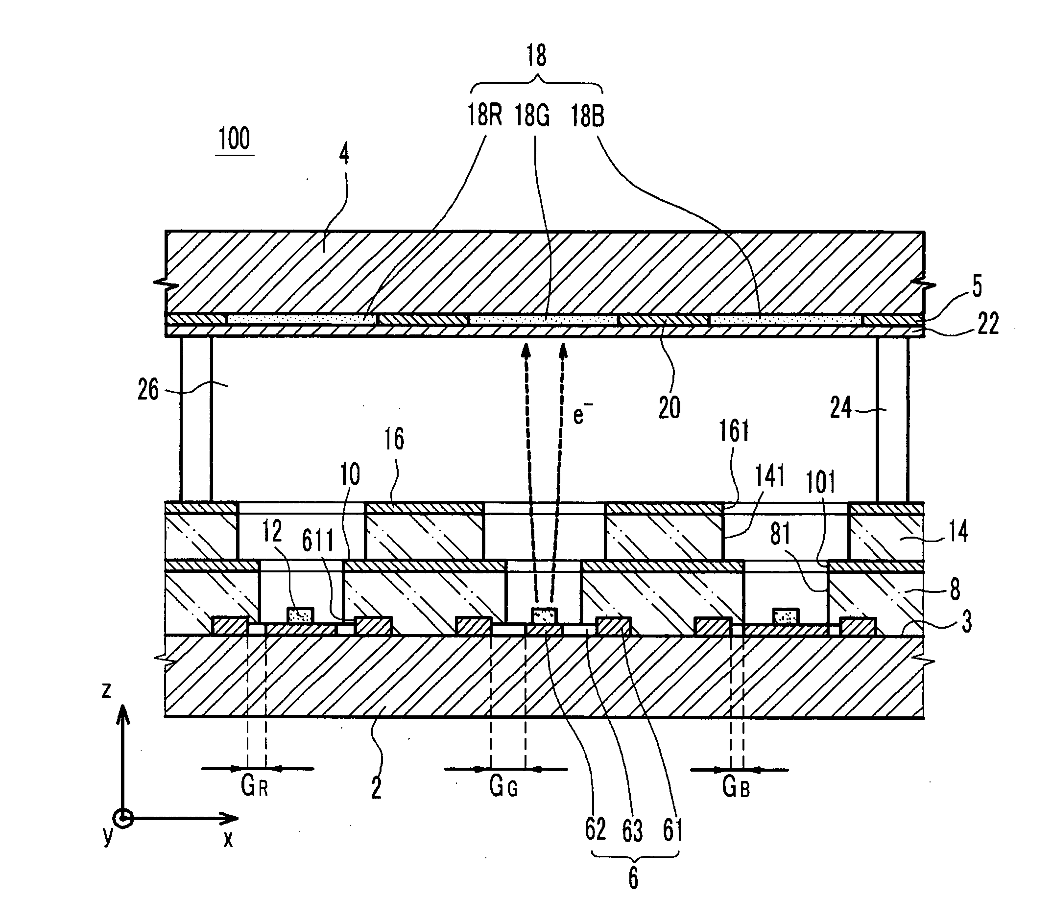
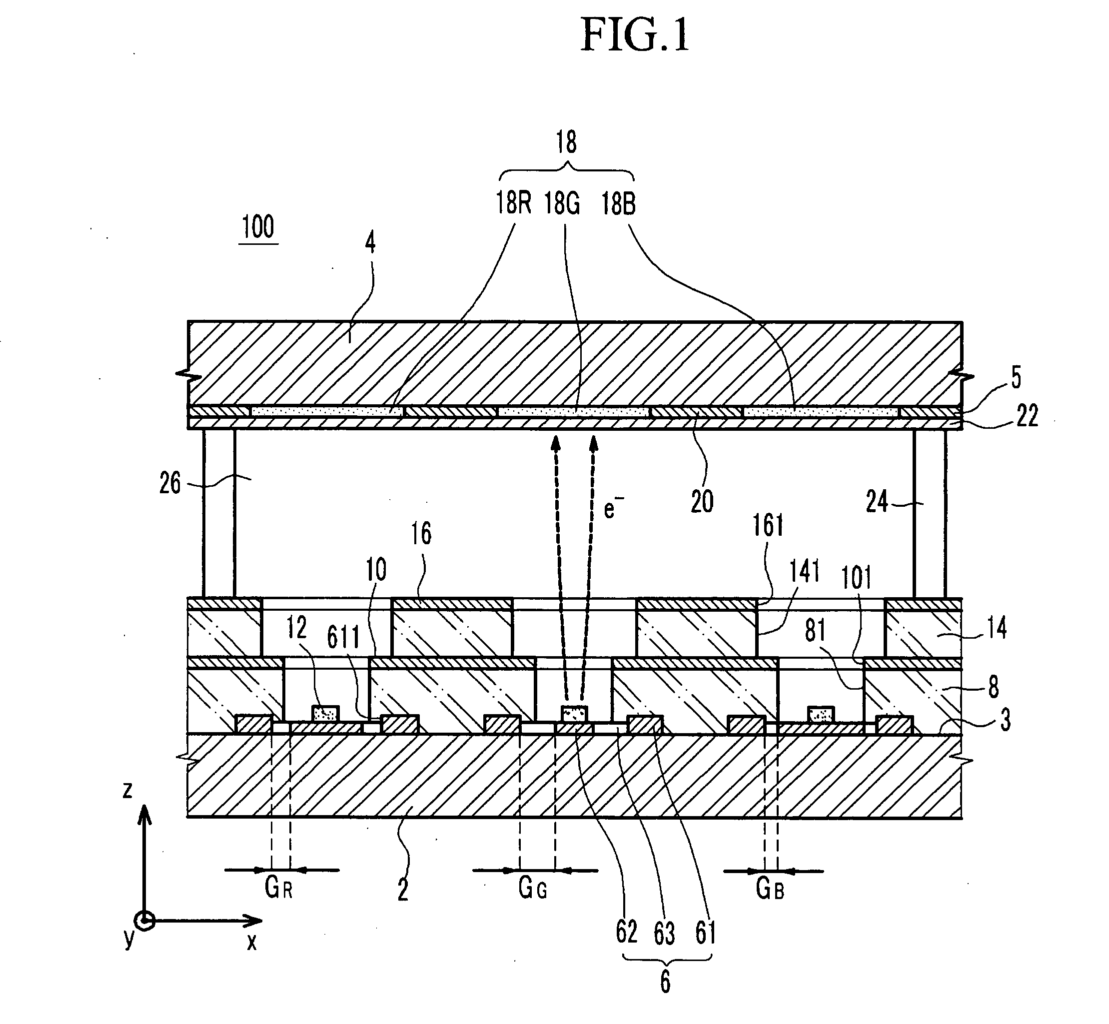
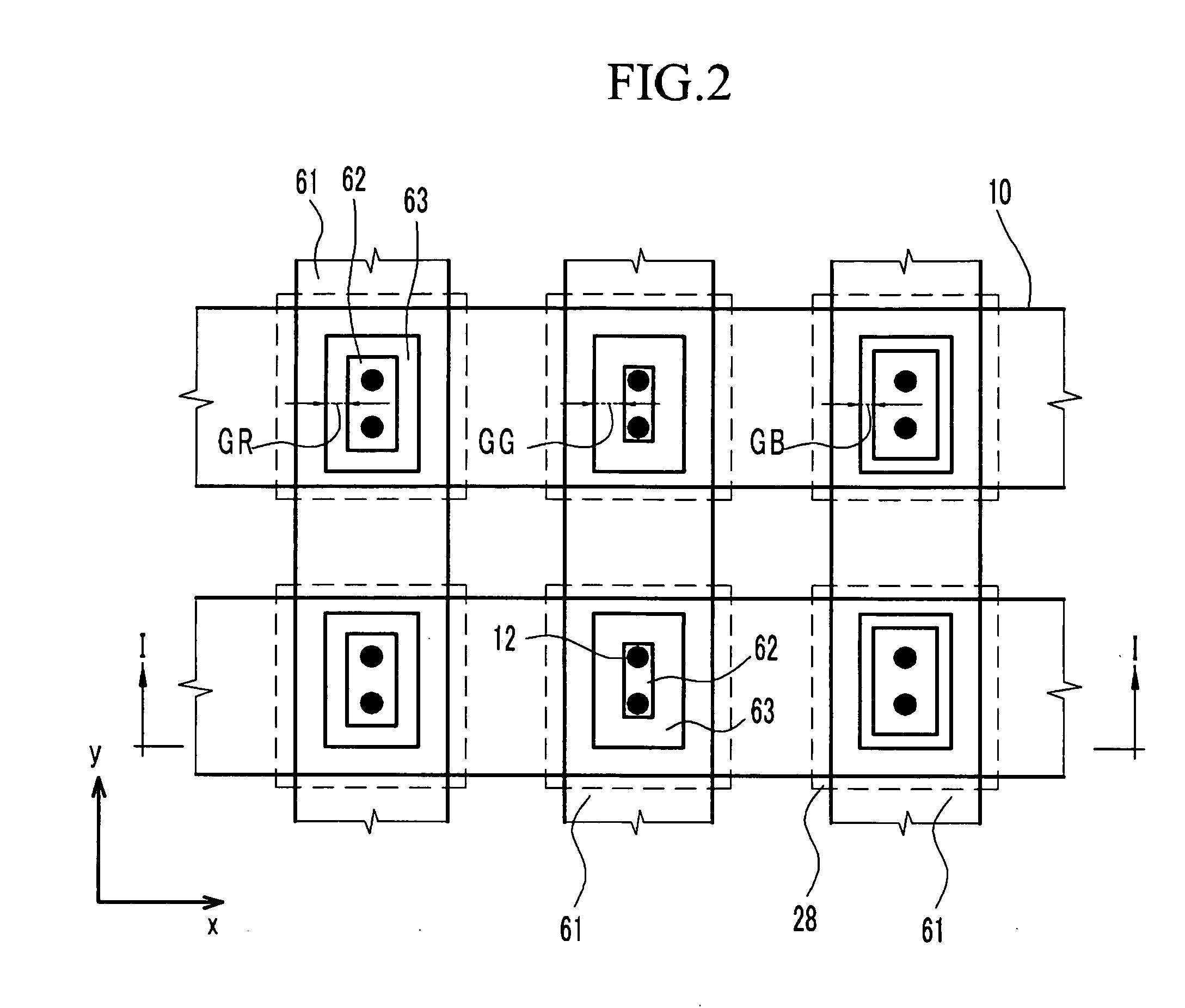
[0025]FIG. 1 is a partial cross-sectional view of an electron emission display device constructed as a first embodiment according to the principles of the present invention, and FIG. 2 is a partial plan view of the electron emission display device illustrated by FIG. 1.
[0026] As shown in FIGS. 1 and 2, electron emission display device 100 is constructed with first and second substrates 2 and 4 facing each other in parallel and spaced apart from each other. First and second substrates 2 and 4 are sealed to each other at the peripheries of first and second substrates 2 and 4 by a sealing member (not shown) to form a vacuum sealed vessel 26, and vessel 26 is evacuated to reach a vacuum of approximately 10−6Torr, thereby constructing a vacuum vessel 26.
[0027] An electron emission element includes electron emission region 12, cathode electrode 7 and gate electrode 10. Arrays of electron emission elements are arranged on surface 3 of first substrate 2 facing second substrate 4 to form an...
second embodiment
[0060]FIG. 3 is a partial cross-sectional view of an electron emission display device 110 constructed as a second embodiment according to the principles of the present invention. In electron emission display device 110 constructed as the present embodiment, resistance layer 73 not only interconnects first and second electrodes 71 and 72, but also contacts electron emission region 12. Consequently, the contact area between electron emission region 12 and cathode electrode 7 is enlarged to thereby increase the amount of electron emissions.
[0061] With a structure constructed according to the principles of the present invention, the width of the resistance layer of the cathode electrode may be controlled to correct the discrepancy in light emission efficiency and luminance between the different-colored phosphor layers, thereby enhancing the screen display quality, and simplifying the driving circuit structure because with this structure it is not necessary to make the correction in the ...
PUM
 Abstract
Description
Claims
Application Information
 - R&D
- Intellectual Property
- Life Sciences
- Materials
- Tech Scout
- Unparalleled Data Quality
- Higher Quality Content
- 60% Fewer Hallucinations
Browse by: Latest US Patents, China's latest patents, Technical Efficacy Thesaurus, Application Domain, Technology Topic, Popular Technical Reports.
© 2025 PatSnap. All rights reserved.Legal|Privacy policy|Modern Slavery Act Transparency Statement|Sitemap|About US| Contact US: help@patsnap.com