Eureka AIR delivers breakthrough ideas for toughest innovation challenges, trusted by R&D personnel around the world.

Wafer guide in wafer cleaning apparatus

Inactive Publication Date: 2007-06-07
SAMSUNG ELECTRONICS CO LTD
View PDF45 Cites 29 Cited by
  • Summary
  • Abstract
  • Description
  • Claims
  • Application Information

AI Technical Summary

Problems solved by technology

While the above-mentioned processes may be used to fabricate semiconductor devices, these processes also generate contaminants.
These contaminants may adhere to the surface of the semiconductor wafer during the manufacturing of the semiconductor device.
When wafers held in a wafer guide are moved from one spot to another, the movement of the wafer guide may produce vibrations that may damage the wafers.
However, inserting wafers deep into the slots of the wafer guide may cause problems.
This increase in the contact surface between the wafer and the slot may lead to a greater possibility of the wafer being damaged.
The damage to the wafer may occur because of scratches forming on the wafer surface in contact with the slot.
Furthermore, as a cleaning solution flows through the scratches, additional defects may also be formed in the wafer.
The problems due to scratches on a wafer are exacerbated when the integration density of a semiconductor device is increased.
This design issue coupled with the problem of an increase in the contact surface between a slot and a wafer may increase the number of scratch related defects in semiconductor wafers.
These problems may decrease the production yield of the semiconductor manufacturing process.
Under certain conditions, when wafers of FIGS. 1 through 3 are loaded in the conventional wafer guide, scratches may occur in the wafer cell areas.
Therefore, it is likely that scratches will occur in the wafer cell area leading to defects in the wafer and to a decrease in the production yield of the semiconductor manufacturing process.
Such a defect caused by the movement of fluids through the wafer cell area may also result in a decrease in the production yield of the semiconductor manufacturing process.

Method used


Image

  • Wafer guide in wafer cleaning apparatus
  • Wafer guide in wafer cleaning apparatus
  • Wafer guide in wafer cleaning apparatus

Examples


Embodiment Construction

[0031] The present invention will now be described with reference to the accompanying drawings, in which preferred embodiments of the invention are shown. However, the invention should not be construed as limited to only the embodiments set forth herein. Rather, the present invention may be embodied in many different forms, and the embodiments are provided so that this disclosure will be thorough and complete, and will fully convey the scope of the invention to those skilled in the art.

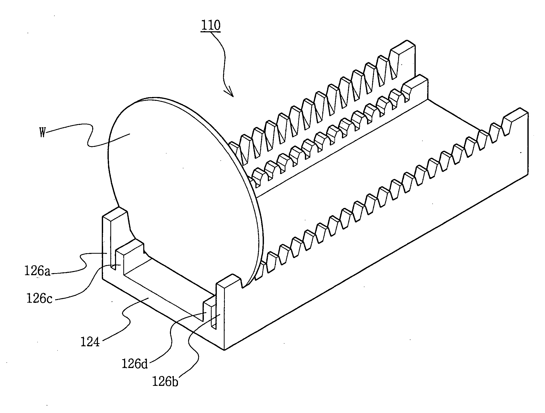
[0032] Various unit processes such as, for example, an ion implantation process, deposition process, and etching process, are performed on a wafer during a semiconductor fabrication process. These unit processes also generate contaminants. These contaminants may include material layers such as a photosensitive layer that is not removed properly during an etching process, or reaction byproducts such as polymers. Furthermore, these polymers adhere to the surface of a semiconductor wafer and may cause v...


PUM


Abstract

A wafer guide in a wafer cleaning apparatus comprises of a lower panel portion. The wafer guide also comprises of a plurality of wafer supporting panel portions, the plurality of wafer supporting panel portions being configured to protrude from at least one side of the lower panel portion and support a wafer. The wafer guide also comprises of a plurality of slot portions, the plurality of slot portions being configured to form at upper ends of the plurality of wafer supporting panel portions and hold the wafer by forming contact with at least a portion of a wafer edge area without forming contact with a wafer cell area.

Description

BACKGROUND OF THE INVENTION [0001] 1. Field of the Invention [0002] The present invention relates generally to semiconductor device manufacturing equipment and, more particularly, to a wafer cleaning apparatus which removes impurities on the surface of a wafer. [0003] This application claims the benefit of Korean Patent Application No. 10-2005-0116945, filed Dec. 2, 2005, in the Korean Intellectual Property Office, the disclosure of which is incorporated herein by reference in its entirety. [0004] 2. Description of the Related Art [0005] Semiconductor devices are manufactured using various processes such as, for example, an impurity ion implantation process, a thin film deposition process, an etching process, and a chemical mechanical polishing (CMP) process. The impurity ion implantation process implants 3B or 5B group impurity ions into a semiconductor. The thin film deposition process forms one or more layers on a semiconductor substrate. The etching process patterns the one or m...

Claims


Application Information

Patent Timeline
IPC IPC(8): A47G19/08
CPCH01L21/67028H01L21/67313H01L21/67326H01L21/304H01L21/683
Inventor SEO, HU-WON
Owner SAMSUNG ELECTRONICS CO LTD
Why Eureka
Eureka Blog
Learn More