Method of forming self-aligned double pattern

a self-aligning, double-shape technology, applied in the direction of basic electric elements, semiconductor devices, electrical equipment, etc., can solve the problems of reaching technical limitations, affecting the size of the device, and the wavelength of the light source used in the photolithography process,

Active Publication Date: 2007-06-28
SAMSUNG ELECTRONICS CO LTD
View PDF8 Cites 156 Cited by
  • Summary
  • Abstract
  • Description
  • Claims
  • Application Information

AI Technical Summary

Problems solved by technology

However, the downscaling of the devices has a limit.
The wavelength of a light source used in a photolithography process, which determines the dimensions of a device, is reaching technical limitations.
However, currently there is no available photoresist, which can absorb a light source having a short wavelength and e...

Method used


Image

  • Method of forming self-aligned double pattern
  • Method of forming self-aligned double pattern
  • Method of forming self-aligned double pattern

Examples


Embodiment Construction

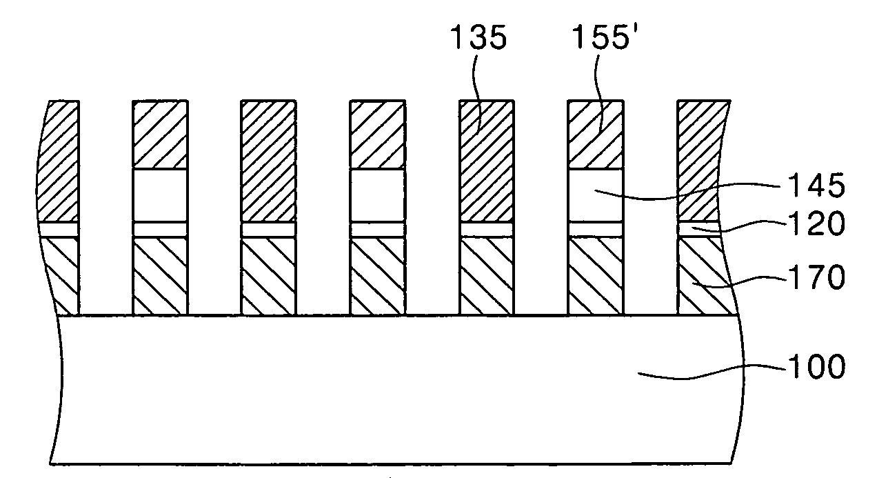
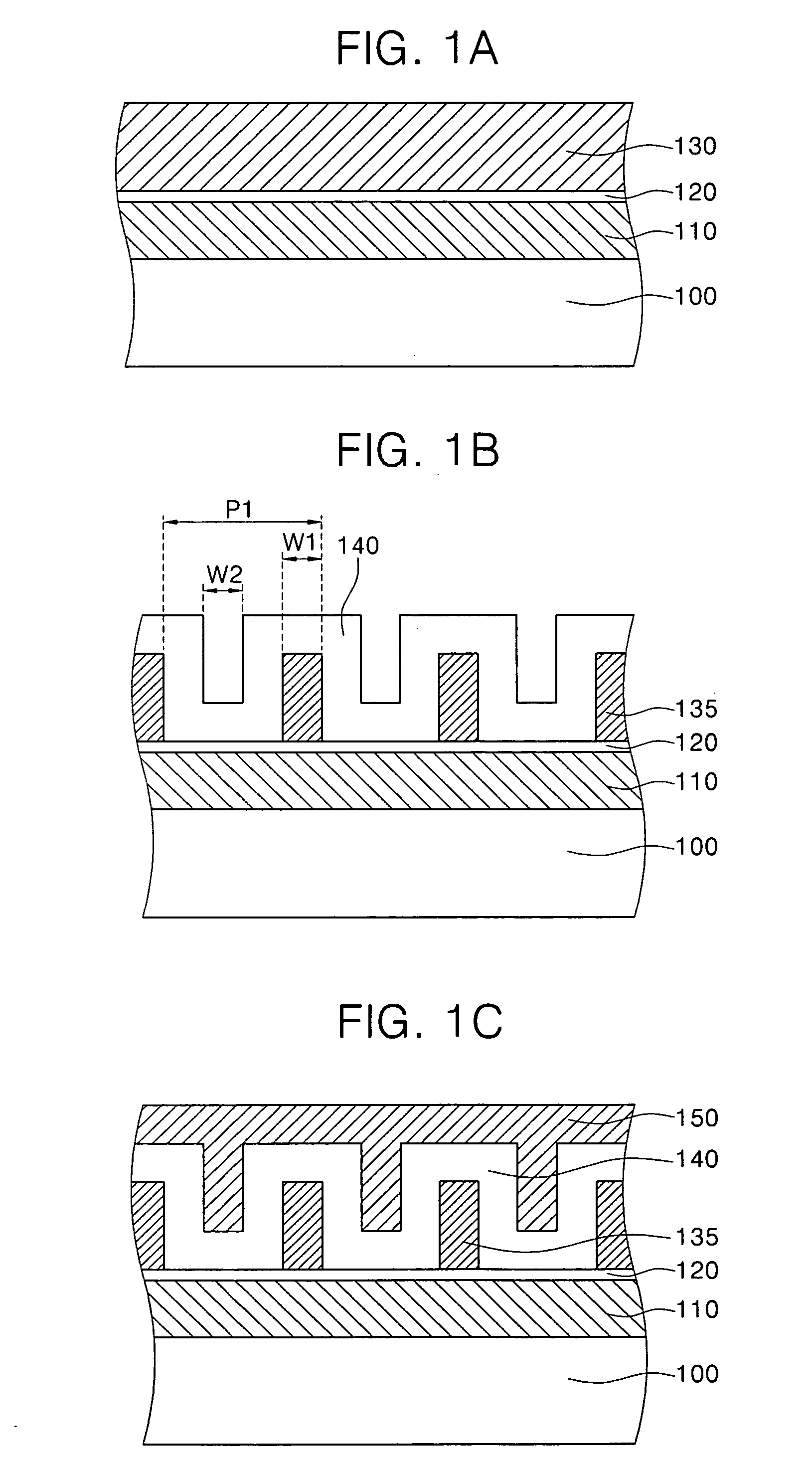
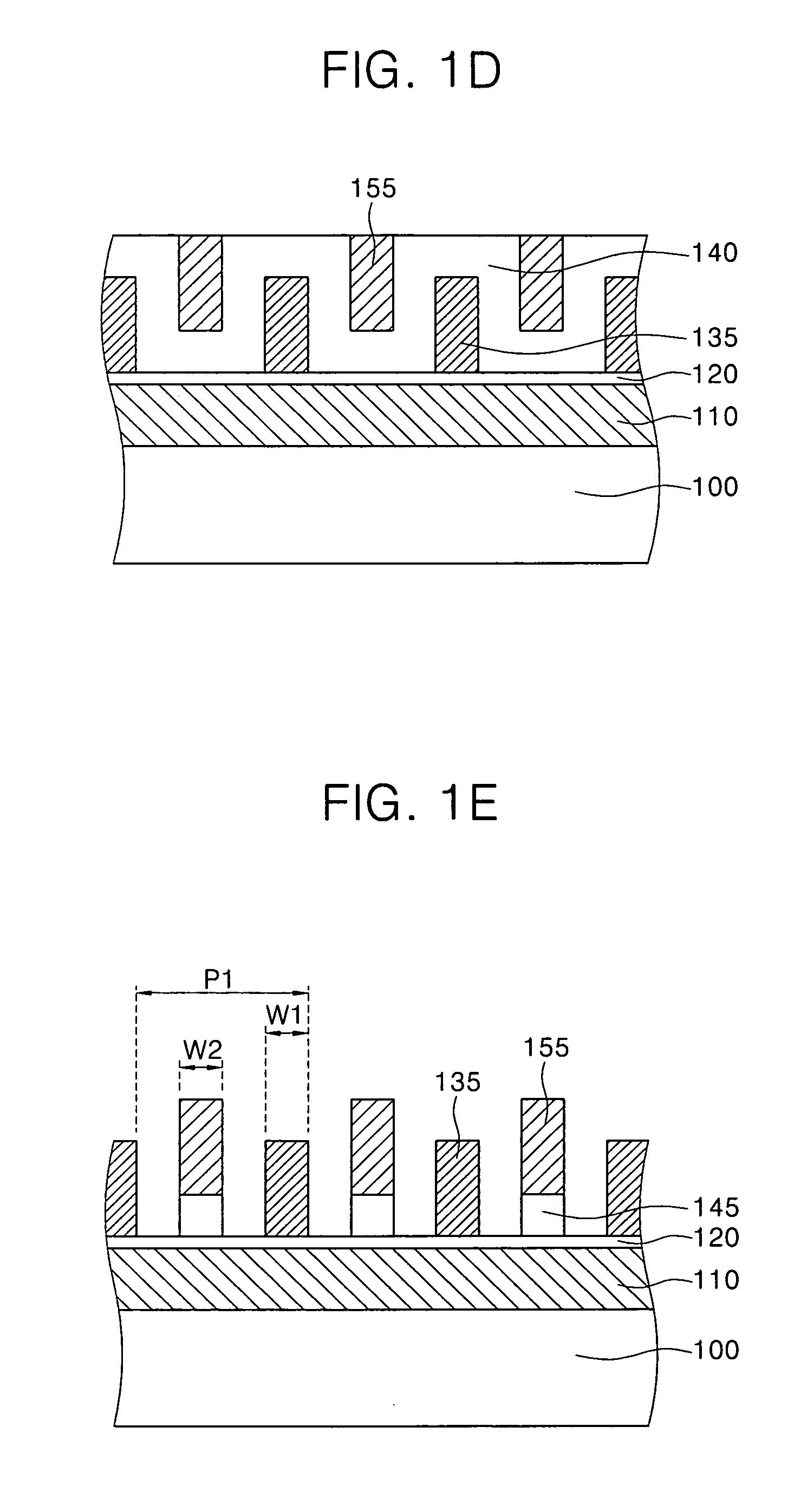
[0019]Example embodiments will now be described more fully hereinafter with reference to the accompanying drawings.

[0020]It will be understood that when an element or layer is referred to as being “on”, “connected to” or “coupled to” another element or layer, it may be directly on, connected or coupled to the other element or layer or intervening elements or layers may be present. In contrast, when an element is referred to as being “directly on,”“directly connected to” or “directly coupled to” another element or layer, there may be no intervening elements or layers present. Like numbers refer to like elements throughout. As used herein, the term “and / or” includes any and all combinations of one or more of the associated listed items.

[0021]It will be understood that, although the terms first, second, third etc. may be used herein to describe various elements, components, regions, layers and / or sections, these elements, components, regions, layers and / or sections should not be ...


PUM


Abstract

Mask patterns used for forming patterns or trenches may include first mask patterns, which may be formed by a typical photolithography process, and second mask patterns, which may be formed in a self-aligned manner between adjacent first mask patterns. A sacrificial layer may be deposited and planarized such that the tops of the first mask patterns and the second mask patterns have planar surfaces. After the planarization of the sacrificial layer, the remaining the sacrificial layer may be removed by an ashing process.

Description

[0001]A claim of priority is made to Korean Patent Application No. 2005-129928, filed on Dec. 26, 2005, the disclosure of which is incorporated herein by reference in its entirety.BACKGROUND OF THE INVENTION[0002]1. Field of the Invention[0003]Example embodiments of the present invention relate to a method of forming a pattern, and more particularly, to a method of forming a self-aligned double pattern.[0004]2. Description of Related Art[0005]Due to an increased demand for highly integrated semiconductor memory devices, techniques of integrating more devices onto a small area have become strongly relied upon. The integration of many devices onto a small area involves downscaling the devices to be formed on a semiconductor substrate. However, the downscaling of the devices has a limit. The wavelength of a light source used in a photolithography process, which determines the dimensions of a device, is reaching technical limitations.[0006]A KrF eximer laser and an ArF eximer laser may ...

Claims


Application Information

Patent Timeline
IPC IPC(8): H01L21/44
CPCH01L21/0337H01L21/0338H01L21/3086H01L21/3088Y10S438/925H01L21/0273
Inventor KWON, BYOUNG-HOYUN, SE-RAHHONG, CHANG-KIYOON, BO-UNCHOI, JAE-KWANGPARK, JOON-SANG
Owner SAMSUNG ELECTRONICS CO LTD
Why Eureka
Try Eureka