In-plane switching mode liquid crystal display and fabrication method thereof

Inactive Publication Date: 2007-07-05
LG DISPLAY CO LTD
View PDF2 Cites 7 Cited by
  • Summary
  • Abstract
  • Description
  • Claims
  • Application Information

AI Technical Summary

Benefits of technology

[0017]An advantage of the present invention is to provide an IPS mode LCD capable of improving an aperture ratio and obtaining a sufficient attachment margin, and its fabrication method.
[0018]Additional features and advantages of the invention will be set forth in the description which follows, and in part will be apparent from the description, or may be learned by practice of the invention. These and other advantages of the invention will be realized and attained by the structure particularly pointed out in the written description and claims hereof as well as the appended drawings.
[0019]To achieve these and other advantages and in accordance with the purpose of the present invention, as embodied and broadly described herein, there is provided an IPS mode LCD including: a plurality of gate lines and a plurality of data lines arranged vertically and horizontally to define a plurality of pixel regions on a first substrate; thin film transistors (TFTs) at each crossing of the gate lines and the data lines and including an active layer, a source electrode and a drain electrode, respectively; a common electrode line arranged substantially parallel to the gate lines; a plurality of first pixel electrodes and first common electrodes and a plurality of second pixel e

Problems solved by technology

As a driving method generally used for the LCD, a twisted nematic (TN) method for driving nematic liquid crystal molecules in a direct

Method used


Image

  • In-plane switching mode liquid crystal display and fabrication method thereof
  • In-plane switching mode liquid crystal display and fabrication method thereof
  • In-plane switching mode liquid crystal display and fabrication method thereof

Examples


Example

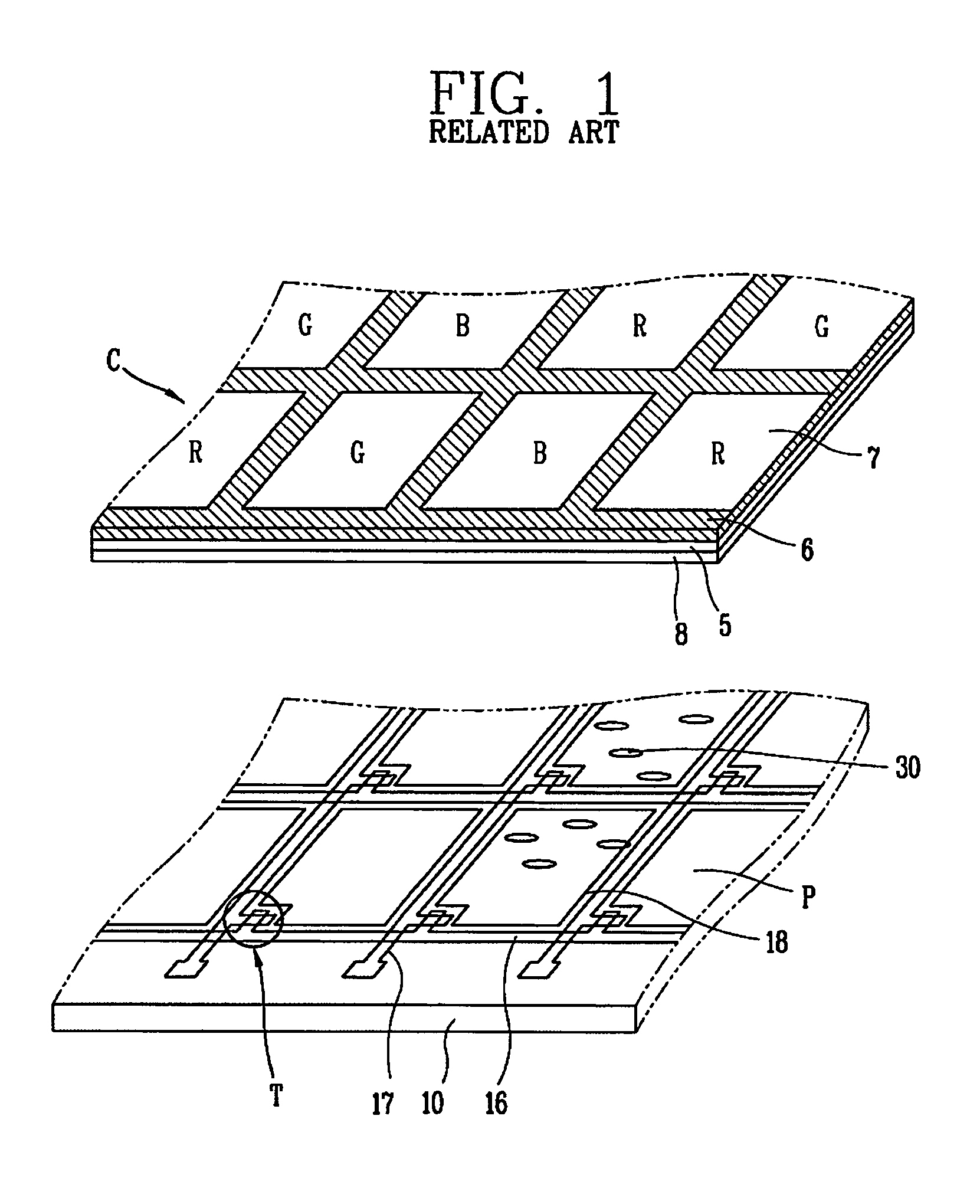
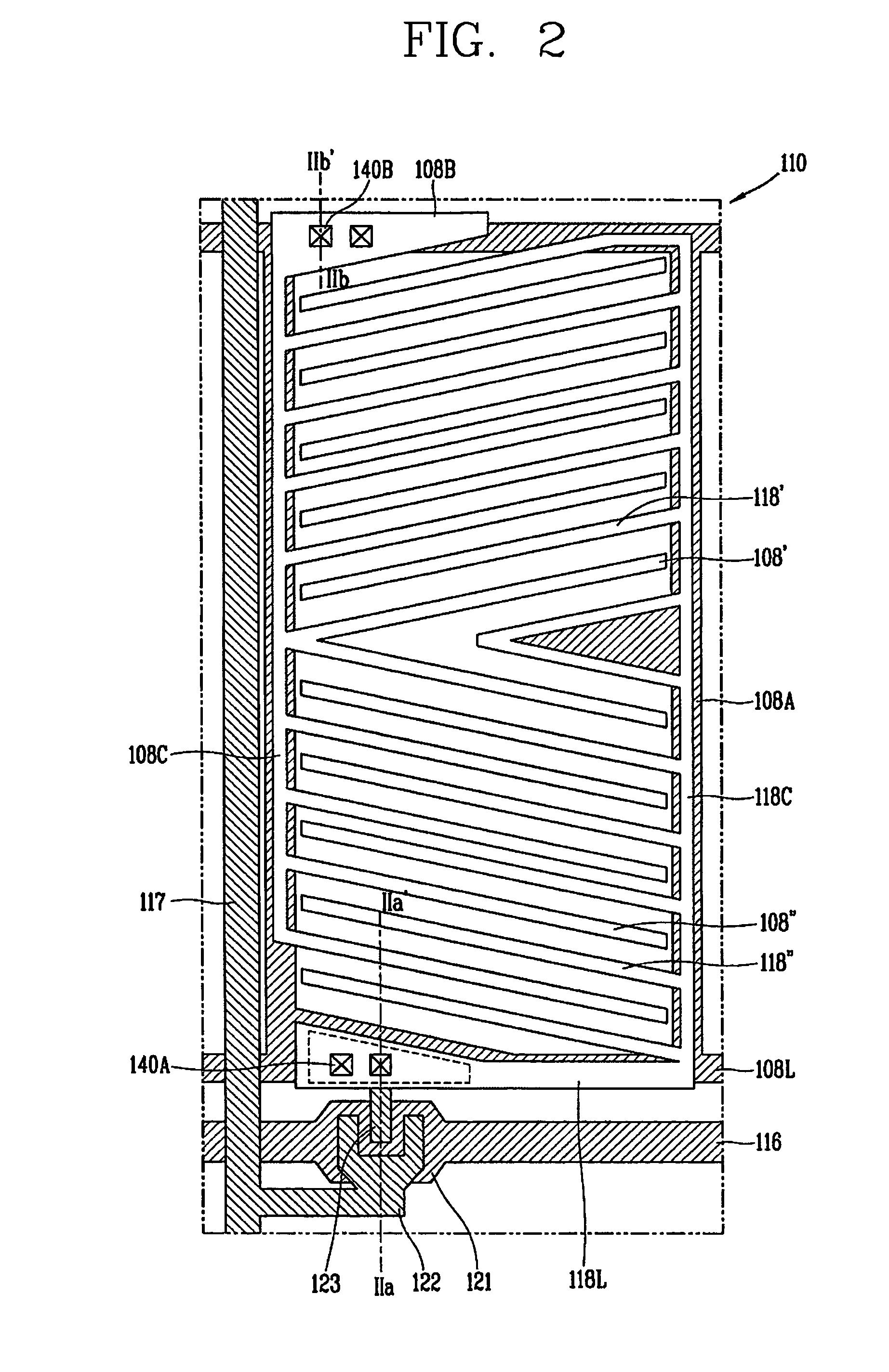
[0034]The LCD according to the first embodiment of the present invention is an IPS mode LCD with an improved viewing angle by more than about 170° by driving liquid crystal molecules in a direction substantially horizontal to substrates. The actual LCD includes the M×N number of pixels as the N number of gate lines and the M number of data lines cross each other. A single pixel is shown in the drawing for the sake of brevity.

[0035]As shown, gate lines 116 and data lines 117 are arranged vertically and horizontally to define pixel regions on an array substrate 110, namely, a transparent glass substrate. Thin film transistors (TFTs), switching elements, are formed at each crossing of the gate lines 116 and the data lines 117.

[0036]Each TFT includes a gate electrode 121 formed as a portion of the gate line 116, a source electrode 122 connected with the data line 117, and a drain electrode 123 connected with pixel electrodes 118′ and 118″ via a pixel electrode line 118L. Each TFT also i...

Example

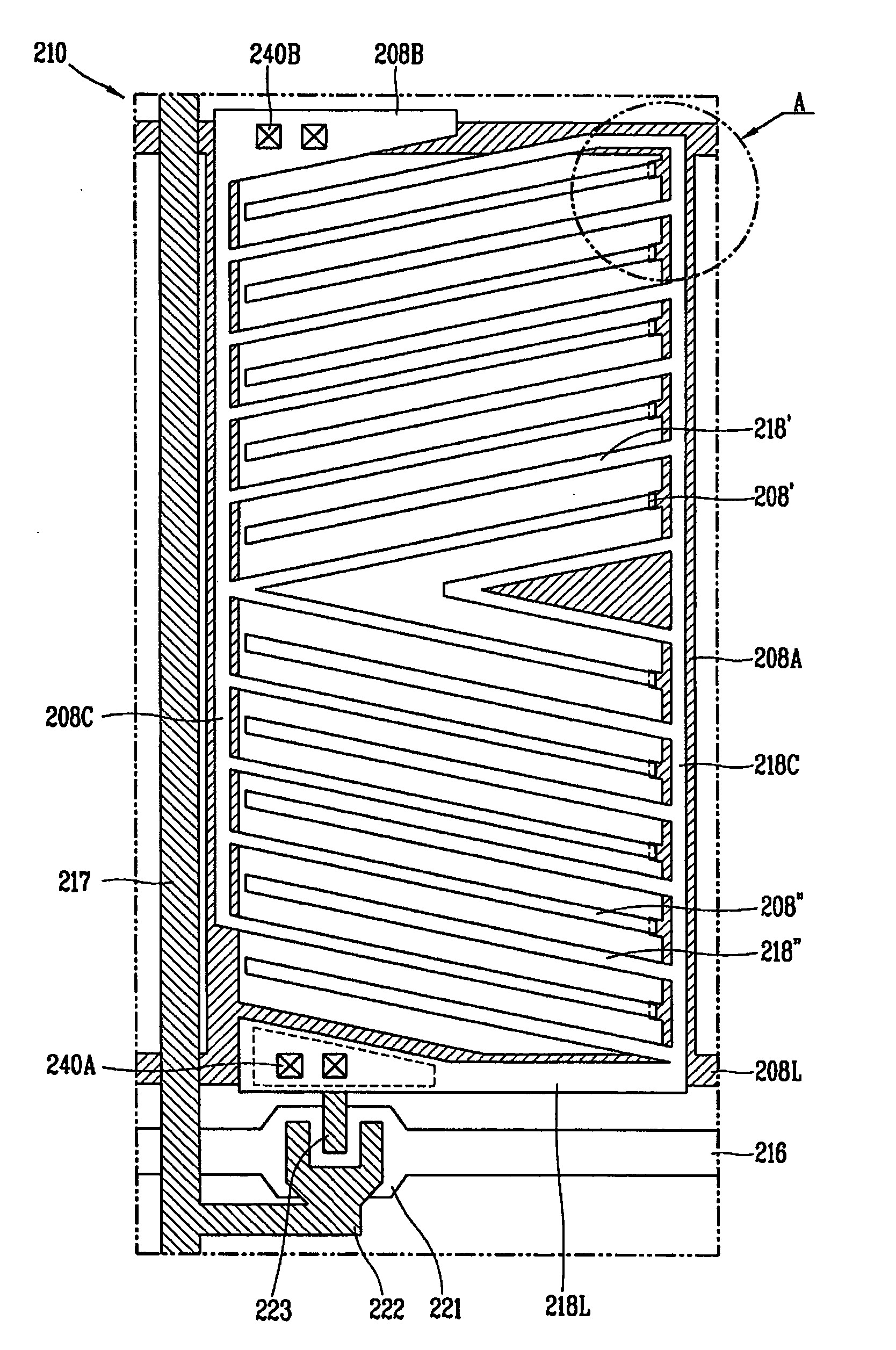
[0048]The array substrate according to the second embodiment of the present invention has the same structure as that of the first embodiment of the present invention, except that an end portion of the common electrode overlaps with a protruded region of the branch.

[0049]As shown, gate lines 216 and data lines 217 are arranged vertically and horizontally to define pixel regions on an array substrate 210, namely, a transparent glass substrate. Thin film transistors (TFTs), switching elements, are formed at each crossing of the gate lines 216 and the data lines 217.

[0050]Each TFT includes a gate electrode 221 formed as a portion of the gate line 216, a source electrode 222 connected with the data line 217, and a drain electrode 223 connected with pixel electrodes 218′ and 218″ via a pixel electrode line 218L. Each TFT also includes a first insulation film (not shown) for insulating the gate electrode 221 and the source / drain electrodes 222 and 223, and an active layer (not shown) for f...

Example

[0057]The array substrate according to the third embodiment of the present invention has the structure as that of the second embodiment of the present invention except that an area where a disclination region is generated is distributed to left and right with respect to a single pixel region in order to minimize a change in luminance according to a defective attachment of the array substrate and a color filter substrate.

[0058]As shown, gate lines 316 and data lines 317 are formed to be arranged vertically and horizontally to define pixel regions on an array substrate 310, namely, a transparent glass substrate. Thin film transistors (TFTs), switching elements, are formed at each crossing of the gate lines 316 and the data lines 317.

[0059]Each TFT includes a gate electrode 321 formed as a portion of the gate line 316, a source electrode 322 connected with the data line 317, and a drain electrode 323 connected with pixel electrodes 318′ and 318″ via a pixel electrode line 318L. Each TF...


PUM


Abstract

An in-plane switching (IPS) mode liquid crystal display (LCD) includes: a plurality of gate lines and data lines arranged vertically and horizontally to define a plurality of pixel regions on a first substrate; thin film transistors (TFTs) at each crossing of the gate and data lines and including an active layer, a source electrode and a drain electrode, respectively; a common electrode line substantially parallel to the gate lines; a plurality of first pixel electrodes and first common electrodes and a plurality of second pixel electrodes and second common electrodes having a tilt angle with respect to the gate lines and alternately disposed on upper and lower portions of the pixel regions to generate an in-plane electric field; and a second substrate attached with the first substrate.

Description

[0001]This application claims the benefit of Korean Patent Application No. 10-2005-0136166, filed on Dec. 30, 2005, which is hereby incorporated by reference for all purposes as if fully set forth herein.BACKGROUND OF THE INVENTION[0002]1. Field of the Invention[0003]The present invention relates to an in-plane switching (IPS) mode liquid crystal display (LCD) and its fabrication method.[0004]2. Discussion of the Related Art[0005]As users' interest in information displays grows and the demand for portable (mobile) information devices increases, research and commercialization of light thin flat panel displays (FPD), which can replace the CRT (Cathode Ray Tube), the existing display device, are actively ongoing.[0006]Among FPDs, the LCD, a device for displaying images by using optical anisotropy of liquid crystal, exhibits excellent resolution and color and picture quality, so it is commonly used for notebook computers or desktop monitors and the like.[0007]The LCD includes a color fi...

Claims


Application Information

Patent Timeline
IPC IPC(8): G02F1/1343
CPCG02F1/134363G02F1/1343
Inventor TAK, YOUNG-MI
Owner LG DISPLAY CO LTD
Why Eureka
Try Eureka