Liquid crystal display panel

Inactive Publication Date: 2012-10-11
HANNSTAR DISPLAY CORPORATION
View PDF12 Cites 7 Cited by
  • Summary
  • Abstract
  • Description
  • Claims
  • Application Information

AI Technical Summary

Benefits of technology

[0009]In the present invention, on the TFT array substrate, the black matrix layer is disposed above the scan lines and the data lines, and between the data lines and the pixel electrodes. The TFT array substrate is later combined with the color filter substrate to form the liquid crystal display. The black matrix layer and the pixel electrodes are all arranged on the TFT array substrate so that the area of the black matrix layer which overlaps the periphery regions of the pixel electrodes for compensating the alignment deviation could be decreased. Accordingly, the redundant light shielding area of the black matrix layer may be reduced in order to increase the aperture ratio of the liquid crystal display panel. Additionally, the black matrix layer has a thickness and a diel

Problems solved by technology

The resultant smaller intervals between neighboring data lines, scan lines and pixel electrod

Method used


Image

  • Liquid crystal display panel
  • Liquid crystal display panel
  • Liquid crystal display panel

Examples


Embodiment Construction

[0016]To provide a better understanding of the present invention, preferred exemplary embodiments will be described in detail herein. The preferred exemplary embodiments of the present invention are illustrated in the accompanying drawings with numbered elements.

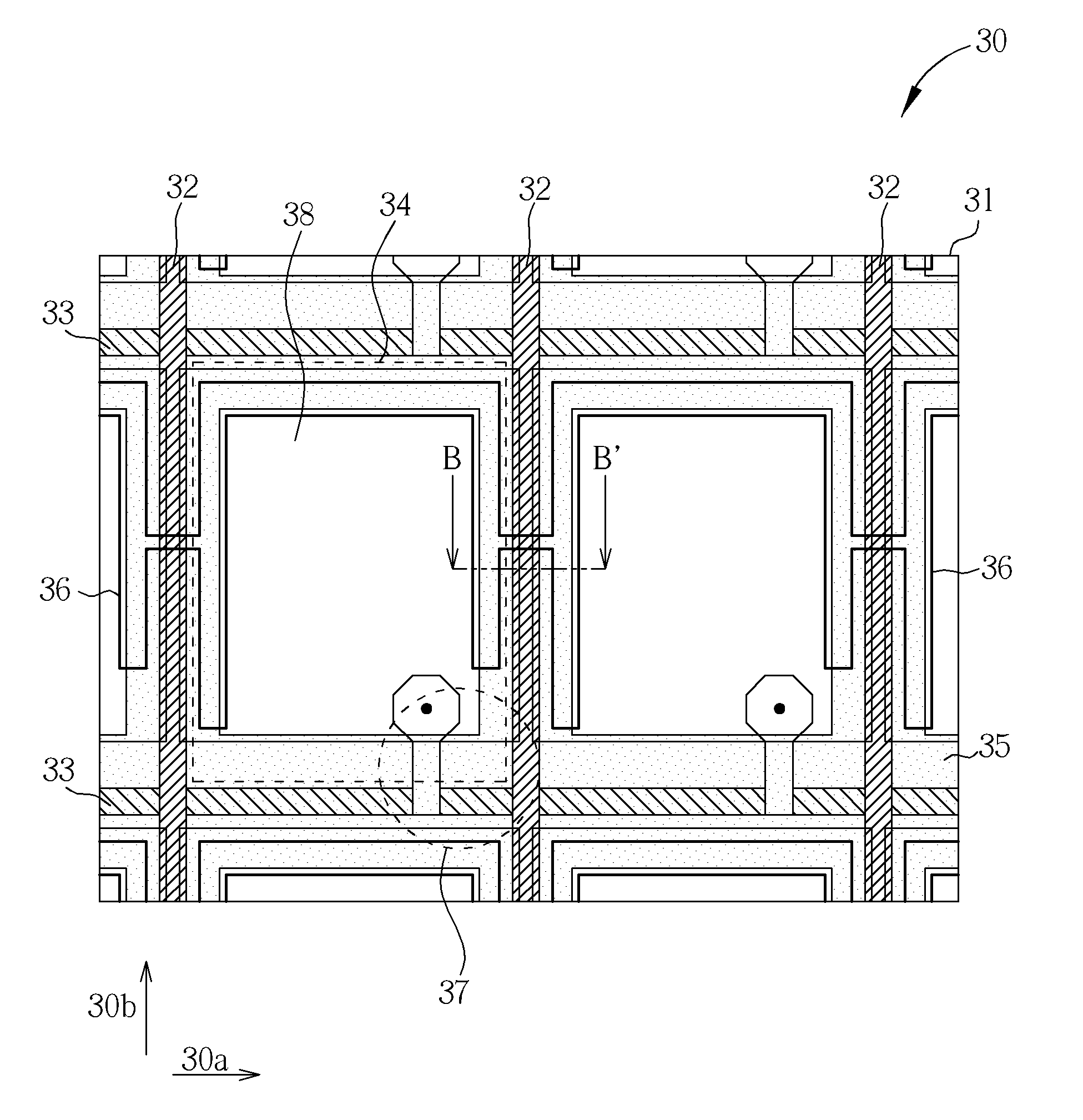
[0017]Please refer to FIG. 3. FIG. 3 illustrates a thin-film transistor (TFT) array substrate 30 according to an exemplary embodiment of the present invention. The TFT array substrate 30 includes a first substrate 31, a plurality of data lines 32, a plurality of scan lines 33, a plurality of pixel regions 34, a black matrix layer 35 and a metal layer 36. The scan lines 33 are arranged parallel to each other along a first direction 30a on the first substrate 31. The data lines 32 are arranged parallel to each other along a second direction 30b on the first substrate 31, and the second direction 30b crosses the first direction 30a. The pixel regions 34 are defined as the regions surrounded by the scan lines 33 and the data lin...


PUM


Abstract

A liquid crystal display includes a thin-film transistor (TFT) array substrate, a color filter substrate and a liquid crystal layer disposed between the TFT array substrate and the color filter substrate. The TFT array substrate includes a first substrate, a plurality of scan lines, a plurality of data lines, a plurality of pixel electrodes and a black matrix layer. The black matrix layer is disposed above the scan lines and the data lines of the TFT array substrate and between the data lines and the pixel electrodes.

Description

BACKGROUND OF THE INVENTION[0001]1. Field of the Invention[0002]The present invention relates to a liquid crystal display panel, and more particularly, to a liquid crystal display panel having a high aperture ratio.[0003]2. Description of the Prior Art[0004]Thin-film transistors (TFTs) are commonly used as active components in active matrix display panels including active matrix liquid crystal displays and active matrix organic electroluminescent display panels. A conventional active matrix liquid crystal display includes a thin-film transistor (TFT) array substrate, a color filter substrate, and a liquid crystal layer interposed between the two.[0005]Please refer to FIG. 1, which illustrates pixel regions of a TFT array substrate according to the prior art. As shown in FIG. 1, a pixel region 10 includes a plurality of data lines 11, a plurality of scan lines 12 crossing the data lines 11 in the form of a grating, a pixel electrode 13 surrounded by the data lines 11 and the scan lin...

Claims


Application Information

Patent Timeline
IPC IPC(8): G02F1/1335
CPCG02F2201/40G02F1/136209
Inventor WU, CHIEN-HAO
Owner HANNSTAR DISPLAY CORPORATION
Why Eureka
Try Eureka