Ltps array substrate

Active Publication Date: 2016-11-24
TCL CHINA STAR OPTOELECTRONICS TECH CO LTD
View PDF2 Cites 11 Cited by
  • Summary
  • Abstract
  • Description
  • Claims
  • Application Information

AI Technical Summary

Benefits of technology

[0026]The present invention provides an LTPS array substrate that has a patternized light shield layer of which the width is increased so as to shield source/drain electrodes and a scan line and partly overlaps a patternized third metal layer that serves as a touch sensing electrode layer, allowin

Problems solved by technology

This increases the operation of the manufacture ther

Method used


Image

  • Ltps array substrate
  • Ltps array substrate
  • Ltps array substrate

Examples


Embodiment Construction

[0032]A clear and complete description will be given to technical solutions of the embodiments of the present invention with reference to the attached drawings of the embodiments of the present invention. However, the embodiments so described are only some, but not all, of the embodiments of the present invention. Other embodiments that are available to those having ordinary skills of the art without the expense of creative effort and endeavor are considered belonging to the scope of protection of the present invention.

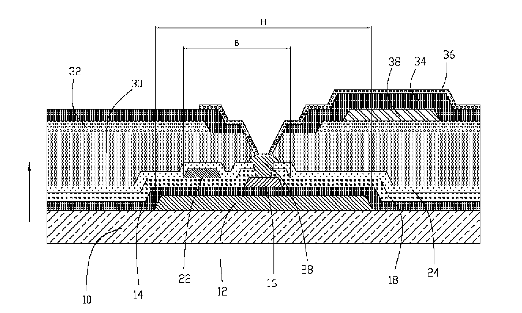
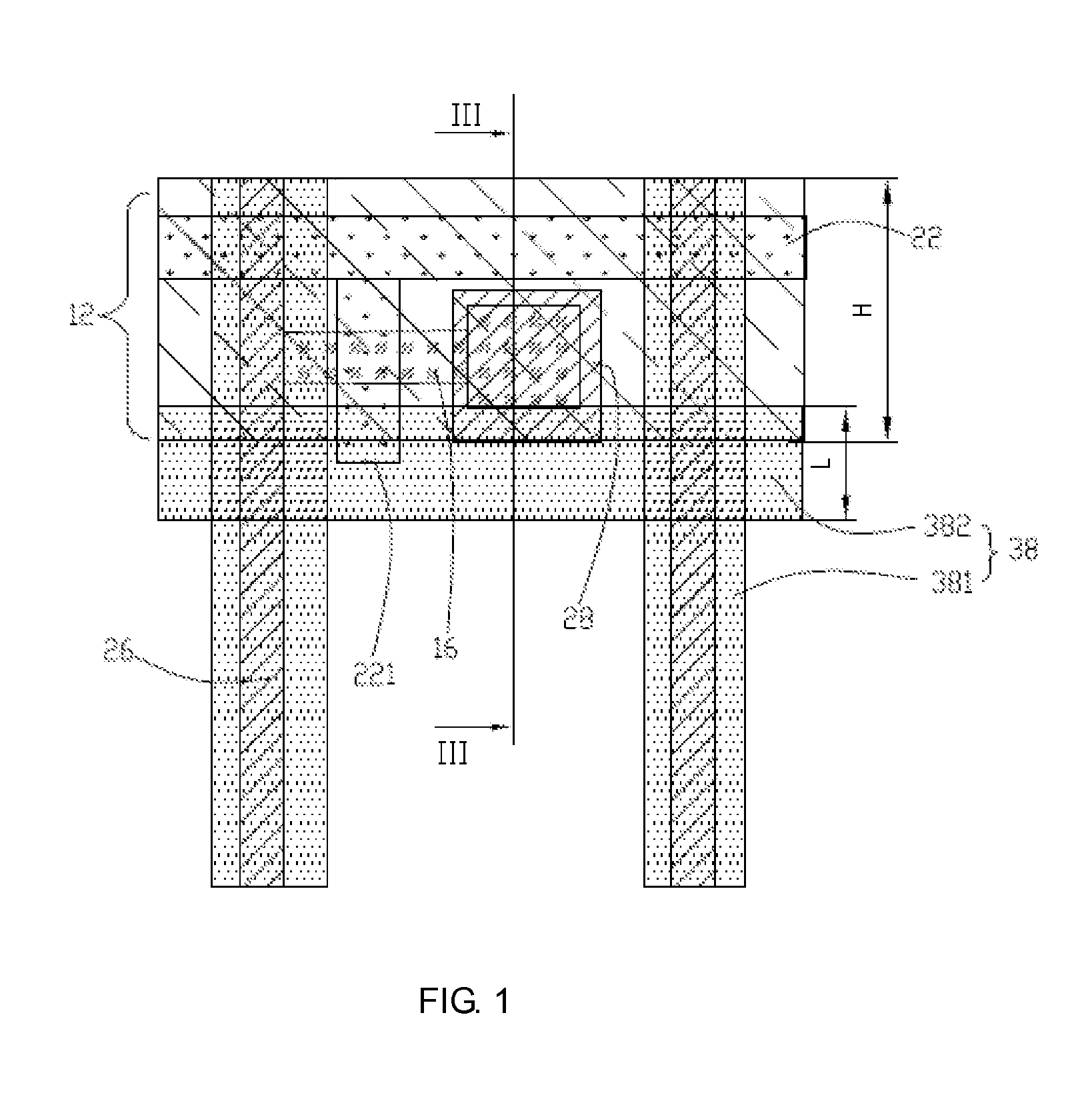
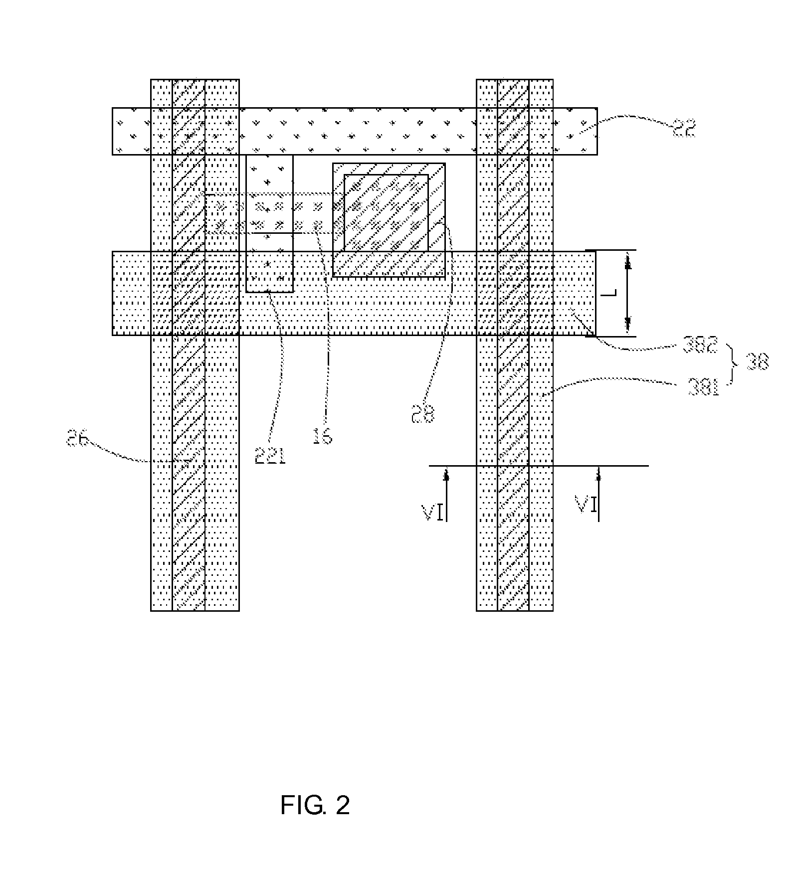
[0033]Referring to FIGS. 1, 2, and 3, the present invention provides a low temperature poly-silicone (LTPS) array substrate, which comprises a plurality of LTPS thin-film transistors and a bottom transparent conductive layer 32, a protective layer 34 formed on the bottom transparent conductive layer 32, and a top transparent conductive layer 36 formed on the protective layer 34. The instant embodiment will be described by taking a single one of the LTPS thin-film tran...


PUM


Abstract

An LTPS array substrate includes a plurality of LTPS thin-film transistors and a bottom transparent conductive layer, a protective layer, and a top transparent conductive layer. Each LTPS thin-film transistor includes a substrate, a patternized light shield layer, a buffering layer, a patternized poly-silicon layer, a gate insulation layer, a gate line, and a common electrode line, an insulation layer, a drain and a source, and a planarization layer that are formed to sequentially stack on each other. The light shield layer covers the scan line and the source/drain. A patternized third metal layer is between the bottom transparent conductive layer and the protective layer and includes a first zone and a second zone intersecting the first zone. The first zone shields the source line. A portion of the second zone overlaps a side portion of the light shield layer that is close to the source/drain electrode.

Description

CROSS REFERENCE TO RELATED APPLICATIONS[0001]This application claims the priority of Chinese Patent Application No. 201410784820.4, entitled “LTPS Array Substrate”, filed on Dec. 16, 2014, the disclosure of which is incorporated herein by reference in its entirety.BACKGROUND OF THE INVENTION[0002]1. Field of the Invention[0003]The present invention relates to the technical field of display screens, and in particular to a low temperature poly-silicon (LTPS) array substrate.[0004]2. The Related Arts[0005]A LTPS (Low Temperature Poly-Silicon) thin-film transistor liquid crystal display is different from a traditional amorphous silicon thin-film transistor liquid crystal display by having electron mobility higher than 200 cm2 / V-sec to effectively reduce the surface area of a thin-film transistor device so as to achieve an increase of aperture ratio and also to reduce the overall power consumption while increasing the brightness of the display. Further, the relatively high electron mobil...

Claims


Application Information

Patent Timeline
IPC IPC(8): H01L27/12G02F1/1333H01L29/45H01L29/786H01L29/51H01L29/49G02F1/1362G02F1/1368
CPCH01L27/1288G02F2202/104G02F1/133345G02F1/136286G02F1/13338G02F1/136277G02F1/1368H01L27/1222H01L27/124H01L29/78633H01L29/78675H01L29/518H01L29/51H01L29/4908H01L29/458G02F2001/136231G02F2001/133357G02F1/136209G02F1/133357G02F1/1333H01L27/12G02F1/1362G02F1/136231
Inventor DU, PENGHU, YUTONG
Owner TCL CHINA STAR OPTOELECTRONICS TECH CO LTD
Why Eureka
Try Eureka