Ball Grid array package structure

Inactive Publication Date: 2007-10-25
POWERTECH TECHNOLOGY
View PDF8 Cites 6 Cited by
  • Summary
  • Abstract
  • Description
  • Claims
  • Application Information

AI Technical Summary

Benefits of technology

[0008]The primary objective of the present invention is to provide a BGA package structure, which can avoid the warpage occurring in the curing process after the encapsulant has been filled into the mold.
[0009]Another objective of the present invention

Problems solved by technology

As shown in FIG. 2, a wBGA package structure is still more fragile, and external force F is still more likely to crack the structure or damage the chip.
A conventional solution is to add an underfill resin into the gap between the package structure and the PCB; thus, the support force is enhanced; however, such a method will add extra cost of the underfill resin and the related process into the fabrication cost.
Another conventional solution is to add extra dummy balls

Method used


Image

  • Ball Grid array package structure
  • Ball Grid array package structure
  • Ball Grid array package structure

Examples


Example

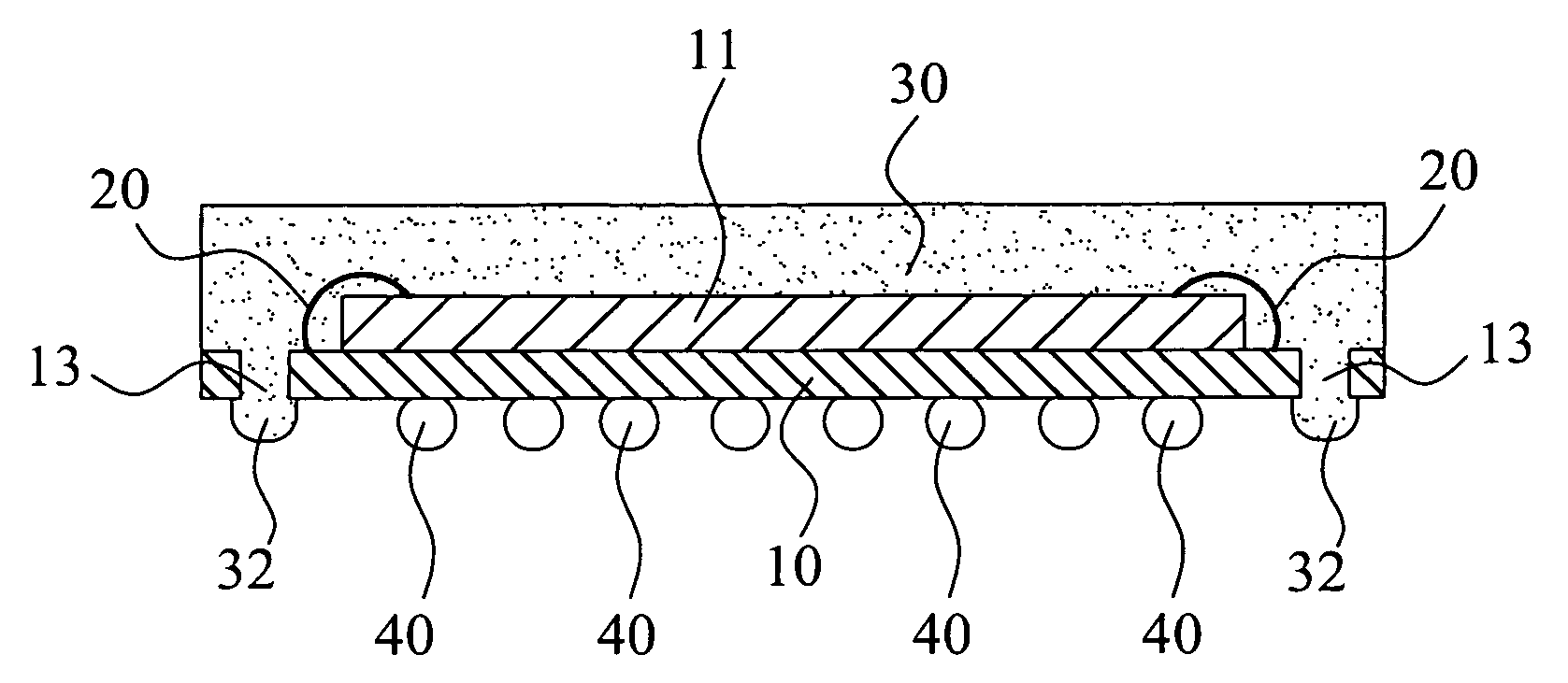
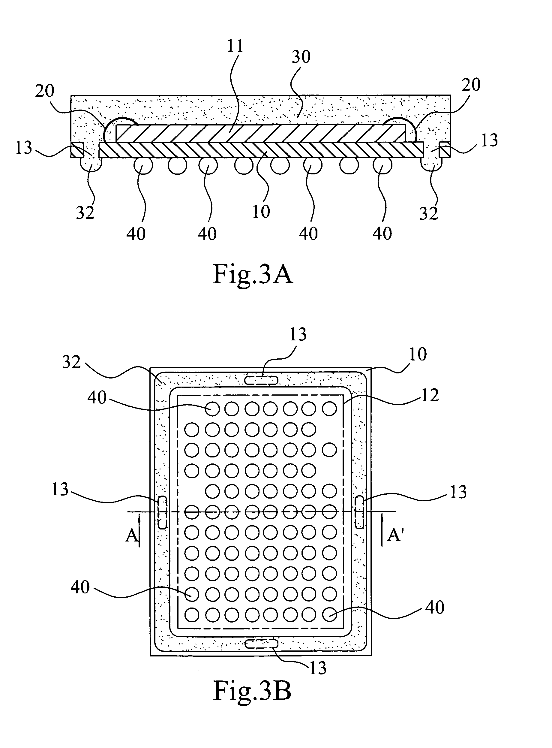
[0017]Refer to FIG. 3A a sectional view schematically showing the BGA package structure according to one embodiment of the present invention. As shown in FIG. 3A, the BGA package structure includes: a substrate 10; a chip 11 arranged on a upper surface of the substrate 10; a plurality of through holes penetrating the substrate 10 and disposed around the perimeter of the chip 11; an encapsulant 30 covering the chip 11 and filling those through holes 13 to form a window-type bump 32 on a lower surface of the substrate 10; and a plurality of conductive balls 40 arranged on the lower surface of the substrate 10, wherein a plurality of electric contacts (not shown in the drawing) are formed on the lower surface of the substrate 10, and the chip 11 is electrically connected with those electric contacts, and those conductive balls 40 are disposed on those electric contacts. In this embodiment, the material of the substrate 10 is selected from the group consisting of polyimide, glass fiber,...


PUM


Abstract

A ball grid array structure includes a substrate, wherein a plurality of electric contacts are arranged on its lower surface; a chip arranged on the upper surface of the substrate and electrically connecting with those electric-connecting points; at least a through hole on the substrate and arranged around the edge of the chip; a molding compound covering the chip and filling the through hole to form a window-type bump on the lower surface of the substrate; and a plurality of conductive balls arranged on those electric-connecting points on the substrate. The present invention utilizes the window-type bump to enhance the structure strength of the substrate to effectively decrease the warpage of package in the curing process and to provide a support to prevent the crack of the package from the external force.

Description

BACKGROUND OF THE INVENTION[0001]1. Field of the Invention[0002]The present invention relates to a semiconductor package structure, particularly to a BGA (Ball Grid Array) package structure.[0003]2. Description of the Related Art[0004]A semiconductor package structure is used to carry an active electronic element, such as a semiconductor chip. Refer to FIG. 1 a sectional view schematically showing a conventional BGA (Ball Grid Array) package structure that mounted on a PCB. As shown in FIG. 1, in the conventional BGA package structure, a chip 110 is arranged on the surface of a substrate 100, and the chip 110 is electrically connected with the substrate 100 via a wire bonding process; a encapsulant 130 is used to cover the chip 110 and conductive wires 120; a plurality of solder balls 140 are arranged in an array on the other side of the substrate 100 and function as I / O (Input / Output) terminals so that the chip 110 carried by the package structure can be electrically connected with...

Claims


Application Information

Patent Timeline
IPC IPC(8): H01L23/02
CPCH01L21/565H01L23/13H01L23/3128H01L23/49816H01L2224/48227H01L2924/01004H01L2924/15311H01L24/48H01L2224/4824H01L2924/00014H01L2224/45099H01L2224/45015H01L2924/207
Inventor FAN, WEN-JENGFANG, LI-CHIHIWATA, RONALD
Owner POWERTECH TECHNOLOGY
Why Eureka
Try Eureka