Chip scale package and fabrication method thereof

Active Publication Date: 2012-02-09
SILICONWARE PRECISION IND CO LTD
View PDF4 Cites 16 Cited by
  • Summary
  • Abstract
  • Description
  • Claims
  • Application Information

AI Technical Summary

Benefits of technology

[0025]Therefore, the present invention mainly involves providing a hard board with a soft layer so as to encapsulate an electronic component with the soft layer while expose the active surface of the electronic component and then performing an RDL process, thereby eliminating the need of a molding process. The hard board can absorb heat stress in the fabrication process so as to avoid the conventional problems caused by directly attaching the electronic component on an adhesive film as in the prior art, such as film-softening caused by heat, electronic component deviation and contamination that lead t

Problems solved by technology

However, the application of the RDL technique or disposing of conductive traces on the chip is limited by the size of the chip or the area of the active surface of the chip.
Particularly, as chips are developed towards high integration and compact size, they do not have enough surface area for mounting of more solder balls for electrical connection to an external device.
However, since the chip is fixed by being attached to the adhesive film, deviation of the chip can easily occur due to film-softening and extension caused by heat, especially in the molding process, thus adversely affecting the electrical connection between the electrode pads of the chip and the wiring layer during the subsequent RDL process.
Further, the use of the adhesive film leads to

Method used


Image

  • Chip scale package and fabrication method thereof
  • Chip scale package and fabrication method thereof
  • Chip scale package and fabrication method thereof

Examples


Example

[0038]FIGS. 4A to 4E′ are cross-sectional views showing a chip scale package and a fabrication method thereof according to a first embodiment of the present invention.

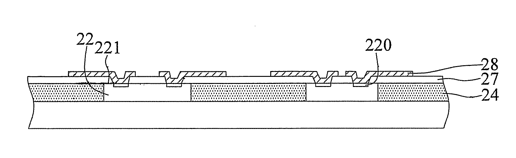
[0039]Referring to FIG. 4A, a plurality of electronic components 22, each having an active surface 221 with a plurality of electrode pads 220 and an inactive surface 222 opposite to the active surface 221, and a hard board 23 with a soft layer 24 disposed thereon are provided. The electronic components 22 can be chips or passive components. The electronic components 22 are adhered to the soft layer 24 via the inactive surfaces 222 thereof by using a pick-up head 25. Each time one or more electronic components 22 can be adhered to the soft layer. The hard board 23 can be made of copper clad laminate (CCL), prepreg (PP), CCL and metal plate laminating board, or PP and metal plate laminating board, which can be peeled off or etched away in a subsequent process. The soft layer 24 can be made of a polymer material, such as ...

Example

Second Embodiment

[0048]FIGS. 5A and 5B are cross-sectional views showing a chip scale package and a fabrication method thereof according to a second embodiment of the present invention. The present embodiment is similar to the first embodiment. A main difference of the present embodiment from the first embodiment is that a die attach film 31 is disposed on the inactive surface 222 of each of the electronic components 22 and the electronic component 22 is adhered to the soft layer 24 through the die attach film 31.

Example

Third Embodiment

[0049]FIG. 6 is cross-sectional view showing a chip scale package and a fabrication method thereof according to a third embodiment of the present invention. Referring to the drawing, the present embodiment is similar to the above-described embodiments. The difference of the present embodiment from the above-described embodiments is that after the step of pressing the electronic components 22, the step of forming the dielectric layer 27, the step of forming the first wiring layer 28 or the step of forming the first solder mask layer 29, at least a conductive through hole 32 is formed in the hard board 23 and the soft layer 24 for electrically connecting the first wiring layer 28. Then, a second wiring layer 28b is formed on the bottom surface of the hard board 23 and electrically connected to the conductive through hole 32; and a second solder mask layer 33 is formed on the bottom surface of the hard board 23 and the second wiring layer 28b and a plurality of openings...


PUM


Abstract

A fabrication method of a chip scale package includes providing electronic components, each having an active surface with electrode pads and an opposite inactive surface, and a hard board with a soft layer disposed thereon; adhering the electronic components to the soft layer via the inactive surfaces thereof; pressing the electronic components such that the soft layer encapsulates the electronic components while exposing the active surfaces thereof; forming a dielectric layer on the active surfaces of the electronic components and the soft layer; and forming a first wiring layer on the dielectric layer and electrically connected to the electrode pads, thereby solving the conventional problems caused by directly attaching a chip on an adhesive film, such as film-softening, encapsulant overflow, warpage, chip deviation and contamination that lead to poor electrical connection between the electrode pads and the wiring layer formed in a subsequent RDL process and even waste product.

Description

BACKGROUND OF THE INVENTION[0001]1. Field of the Invention[0002]The present invention relates generally to semiconductor packages and fabrication methods thereof, and more particularly, to a chip scale package and a fabrication method thereof.[0003]2. Description of Related Art[0004]A chip scale package (CSP) is characterized in that the package size is equivalent to the size of the chip that is disposed in the package. U.S. Pat. No. 5,892,179, U.S. Pat. No. 6,103,552, U.S. Pat. No. 6,287,893, U.S. Pat. No. 6,350,668 and U.S. Pat. No. 6,433,427 disclose a conventional CSP structure, wherein a build-up structure is directly formed on a chip without using a chip carrier, such as a substrate or a lead frame, and a redistribution layer (RDL) technique is used to accomplish a redistribution of the electrode pads of the chip to a desired pattern.[0005]However, the application of the RDL technique or disposing of conductive traces on the chip is limited by the size of the chip or the area ...

Claims


Application Information

Patent Timeline
IPC IPC(8): H01L25/07H01L23/48H01L21/98
CPCH01L24/96H01L2224/73267H01L25/50H01L2224/04105H01L2224/13022H01L2224/13099H01L2224/16221H01L2224/211H01L2224/221H01L2224/83191H01L2224/92244H01L2225/1035H01L2225/1058H01L2924/01029H01L2924/01082H01L2924/12H01L2924/14H01L25/105H01L2224/0401H05K3/4644H01L2224/96H01L2224/12105H01L2224/05548H01L21/561H01L24/19H01L24/20H01L2924/01005H01L2924/01006H01L2924/01033H01L2924/014H01L2924/3511H01L2224/02379H05K1/185H01L2224/19H01L2224/11H01L2924/00014
Inventor CHANG, CHIANG-CHENGKE, CHUN-CHIHUANG, CHIEN-PING
Owner SILICONWARE PRECISION IND CO LTD
Why Eureka
Try Eureka