
Semiconductor device and manufacturing method for the same
- Summary
- Abstract
- Description
- Claims
- Application Information
AI Technical Summary
Benefits of technology
Problems solved by technology
Method used
Image

Examples
first embodiment
[0047] [First Embodiment]
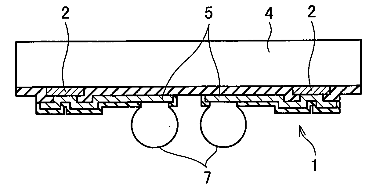
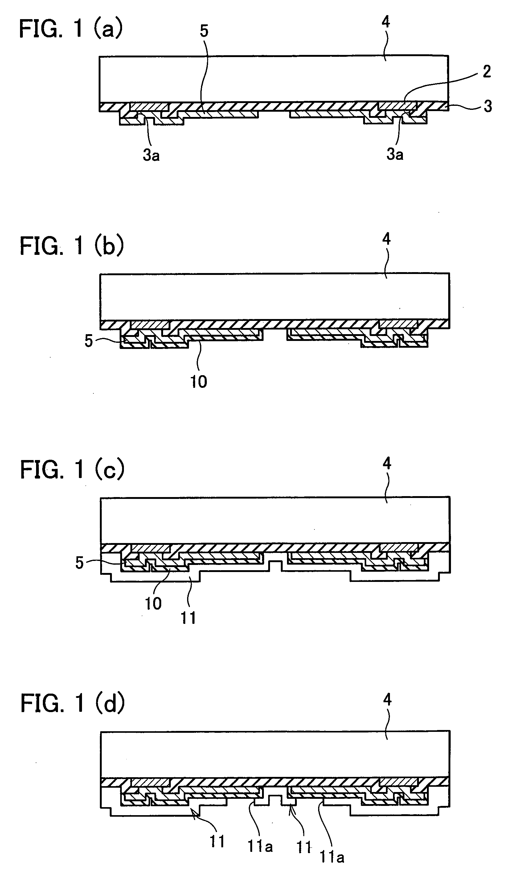
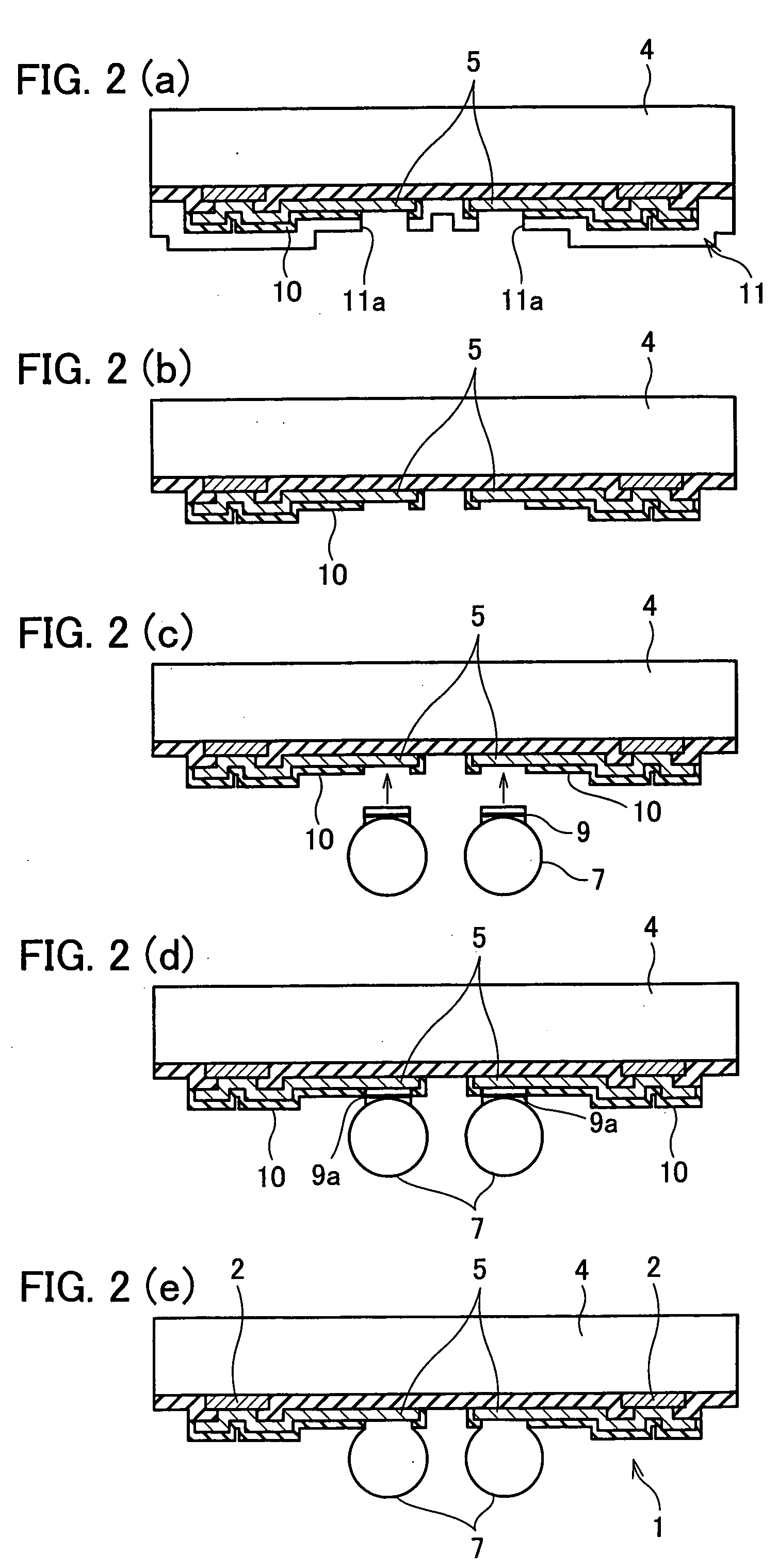
[0048] FIGS. 1(a) through 2(e) are cross-sectional views illustrating some of the processing steps of a manufacturing method of semiconductor device according to First Embodiment of the present invention. These figures each show a cross section in manufacturing of one of plural semiconductor chips (semiconductor devices) formed on a silicon wafer (substrate) 4. The following explains the manufacturing method according to First Embodiment of the present invention with reference to FIGS. 1(a) through 2(e).
[0049]FIG. 1(a) shows a silicon wafer 4 on which an electric circuit, such as an integrated circuit, and electrode pads for allowing external electrical conduction of the electric circuit are formed through an electric circuit forming step (not shown). The silicon wafer 4 further includes a protection film 3 with an opening on a desired one of the electrode pads 2 through a protection film forming step (not shown).
[0050] The silicon wafer 4 further includes...
second embodiment
[0074] [Second Embodiment]
[0075] FIGS. 5(a) through 6(e) are cross-sectional views illustrating some of the processing steps of a manufacturing method of semiconductor device according to Second Embodiment of the present invention. These figures each show a cross section in manufacturing of one of plural semiconductor chips formed on a silicon wafer 4. The following explains the manufacturing method according to Second Embodiment of the present invention with reference to FIGS. 5(a) through 6(e).
[0076]FIG. 5(a) shows a silicon wafer 4 on which an electric circuit element, such as an integrated circuit, and electrode pads for allowing external electrical conduction of the electric circuit are formed through an electric circuit forming step (not shown). The silicon wafer 4 further includes a protection film 3 with an opening on a desired one of the electrode pads 2 through a protection film forming step (not shown). Further, a wiring pattern 5 as copper re-wiring is formed across the...
third embodiment
[0089] [Third Embodiment]
[0090] FIGS. 7(a) through 8(d) are cross-sectional views illustrating a semiconductor device and a manufacturing method thereof according to Third Embodiment of the present invention. These figures each show a cross section of one of plural semiconductor chips 1 formed on a silicon wafer 4. The following explains the manufacturing method according to Third Embodiment of the present invention with reference to FIGS. 7(a) through 8(d).
[0091]FIG. 1(a) shows a silicon wafer 4 on which an electric circuit, such as an integrated circuit, and electrode pads for allowing external electrical conduction of the electric circuit are formed through an electric circuit forming step (not shown). The silicon wafer 4 further includes a protection film 3 with an opening on a desired one of the electrode pads 2 through a protection film forming step (not shown). The silicon wafer 4 further includes a wiring pattern 5 as copper re-wiring that is electrically conducted and form...
PUM
| Property | Measurement | Unit |
|---|---|---|
| Area | aaaaa | aaaaa |
| Wettability | aaaaa | aaaaa |
Abstract
Description
Claims
Application Information