Semiconductor device and method for manufacturing same

Active Publication Date: 2007-03-29
RENESAS ELECTRONICS CORP
View PDF9 Cites 67 Cited by
  • Summary
  • Abstract
  • Description
  • Claims
  • Application Information

AI Technical Summary

Benefits of technology

[0011] In the semiconductor device according to the above-described aspect of the present invention, the protruding portion protruding in the direction along the surface of the semiconductor substrate toward the interior of the through electrode is provided in the vicinity of the back surface of the semiconductor substrate, and the protruding portion is in contact with the through electrode. Consequently, the through electrode is supported by the protruding portion in the side of the back surface of the semiconductor substrate, so that the falling off of the through electrode from the substrate can be avoided. Further, the semiconductor device according to the above-described aspect of the present invention is configured to be provided with the through electrode, which can be manufactured from the side of the back surface. Consequently, according to the aspect of the present invention, a falling off of the through electrode from the side of the back surface can be effectively prevented without decreasing a reliability of the semiconductor device.
[0012] In addition, since the annular cylindrical insulating film is provided in the periphery of the through electrode in the semiconductor device according to the above-described aspect of the present invention, an electrical insulation can be provided in the periphery of the through electrode and a parasitic capacitance can be reduced. In addition, since the electrical insulation is ensured in the periphery of the through electrode, a closely packing of the through electrodes can be achieved.
[0013] According to another aspect of the present invention, there is provided a method for manufacturing a semiconductor device, comprising: forming an annular cylindrical insulating film, by selectively removing the semiconductor substrate from a side of a device-forming surface of the semiconductor substrate to form an annular cylindrical concave portion, then filling an insulating film in an interior of the annular cylindrical concave portion and removing portions of the insulating film located outside of the annular cylindrical concave portion; forming a predetermined semiconductor device in the device-forming surface; reducing

Problems solved by technology

Consequently, it is difficult to achieve closely packing of the through electrodes.
In such case, when a procedure of forming the through electrode before forming the device is employed, better heat resistance is required for a material for forming the electrode, and thus a range of choice for the electrode material may often be limited.
Further, when a procedure of

Method used


Image

  • Semiconductor device and method for manufacturing same
  • Semiconductor device and method for manufacturing same
  • Semiconductor device and method for manufacturing same

Examples


first embodiment

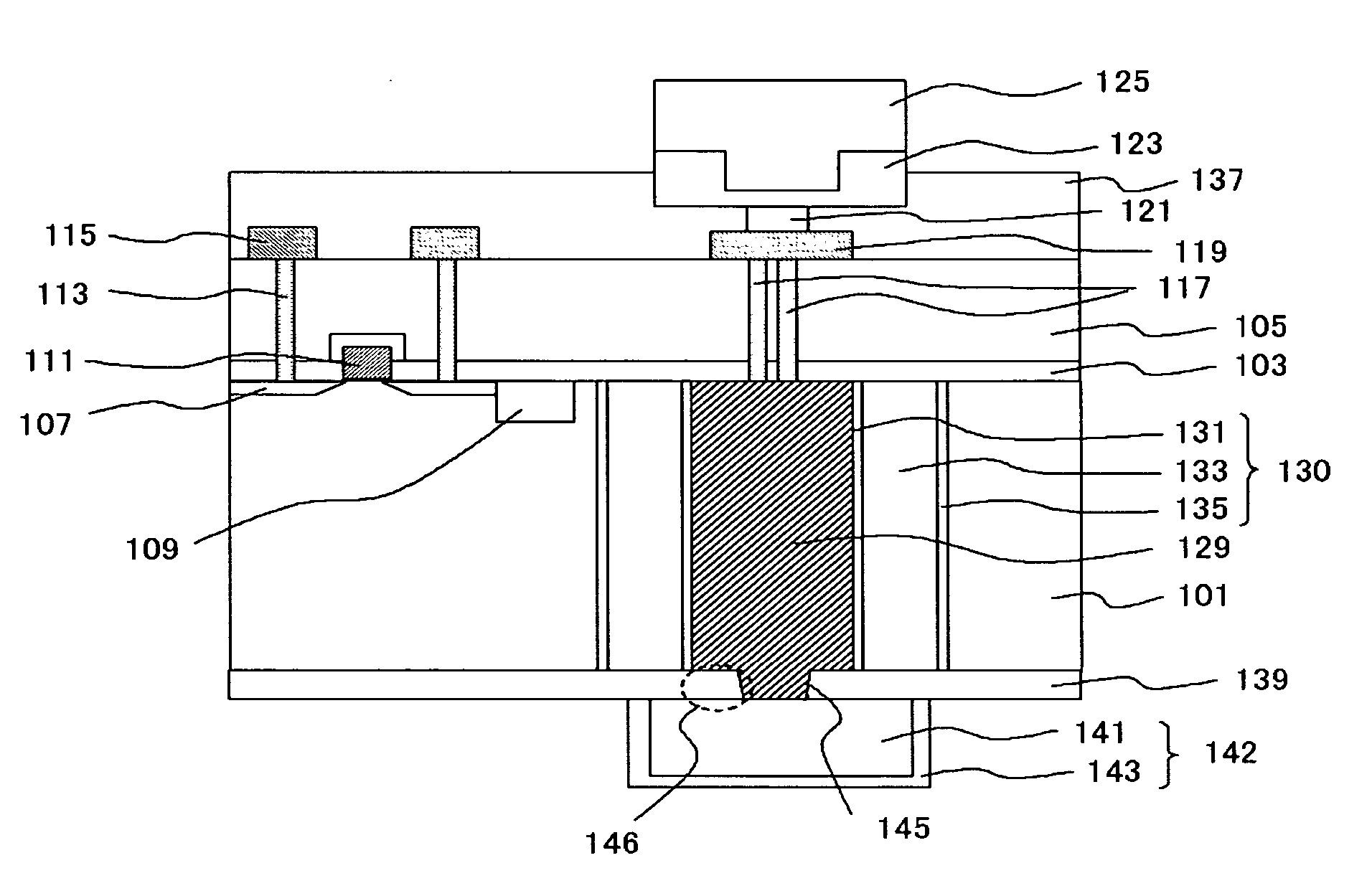
[0048]FIG. 1 is a cross-sectional view, illustrating a configuration of a semiconductor device of the present embodiment. A semiconductor device 100 shown in FIG. 1 includes: a semiconductor substrate (silicon substrate 101); a through electrode 129 extending through the silicon substrate 101; an annular cylindrical insulating film (first insulating ring 130) provided in a circumference of a side surface of the through electrode 129 and extending through the semiconductor substrate 101; and a protruding portion 146, being provided at least in the vicinity of a back surface of a device-forming surface of the semiconductor substrate 101 so as to contact with the through electrode 129, and protruding in a direction along the surface of the semiconductor substrate 101 toward an interior of the through electrode 129. The semiconductor device 100 further includes a back surface insulating film 139 provided so as to contact with the back surface of the silicon substrate 101.

[0049] The pro...

second embodiment

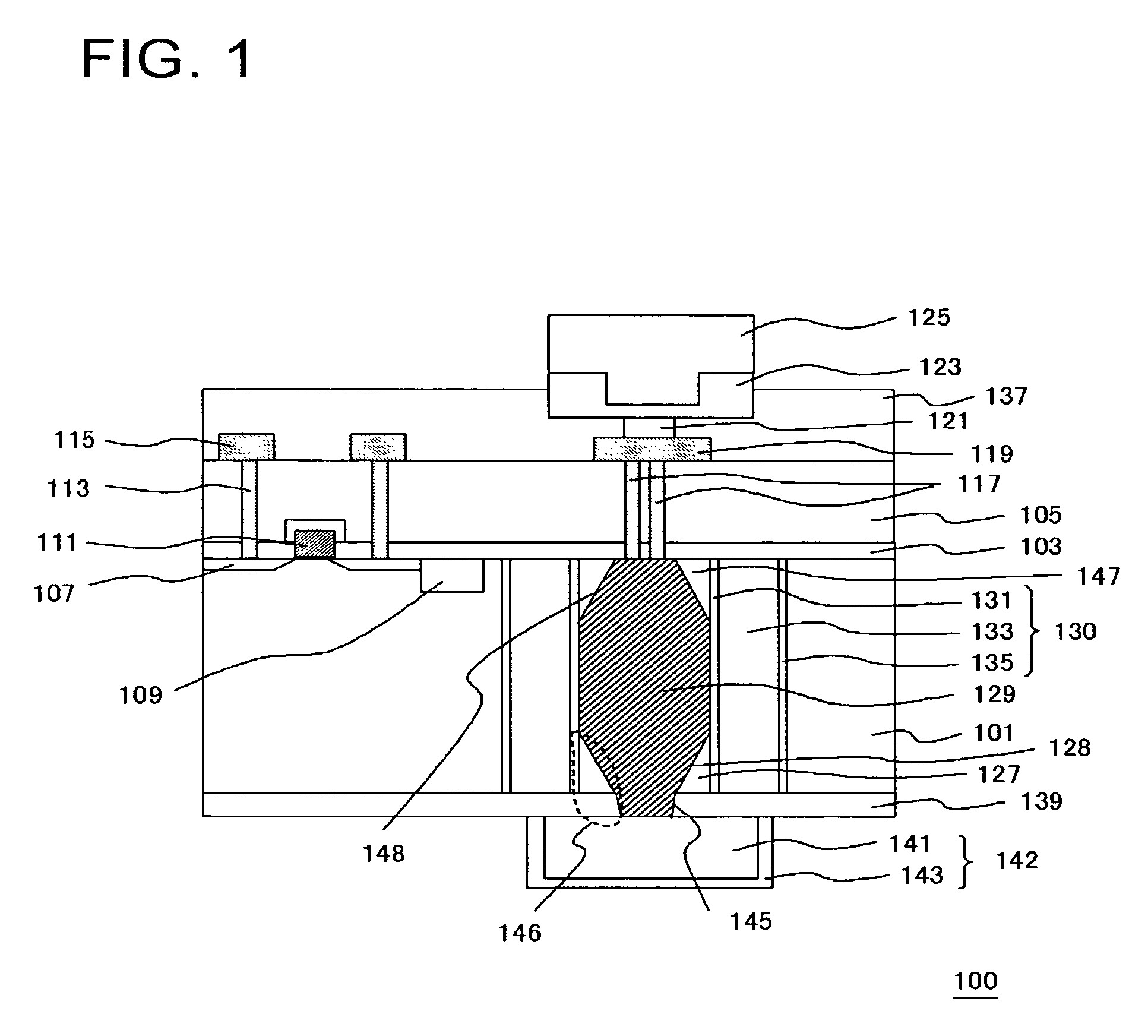
[0111]FIG. 2 is a cross-sectional view, illustrating a configuration of a semiconductor device of the present embodiment. Fundamental configuration of the semiconductor device shown in FIG. 2 is similar to the semiconductor device 100 illustrated in FIG. 1, except that: the silicon substrate remaining portion 147 is not provided; and in the vicinity of the device-forming surface of the silicon substrate 101, the portion of the silicon substrate 101 located in the interior of the first insulating ring 130 are all removed, and a Cu film is embedded in the removed region. More specifically, in FIG. 2, a region of the remained silicon substrate 101 is selectively provided in the vicinity of the back surface of the silicon substrate 101 in a region inside of the first insulating ring 130.

[0112] Since the protruding portion, which is composed of the tapered surface 145 and the silicon substrate remaining portion 127, is also provided at least in the vicinity of the back surface of the si...

third embodiment

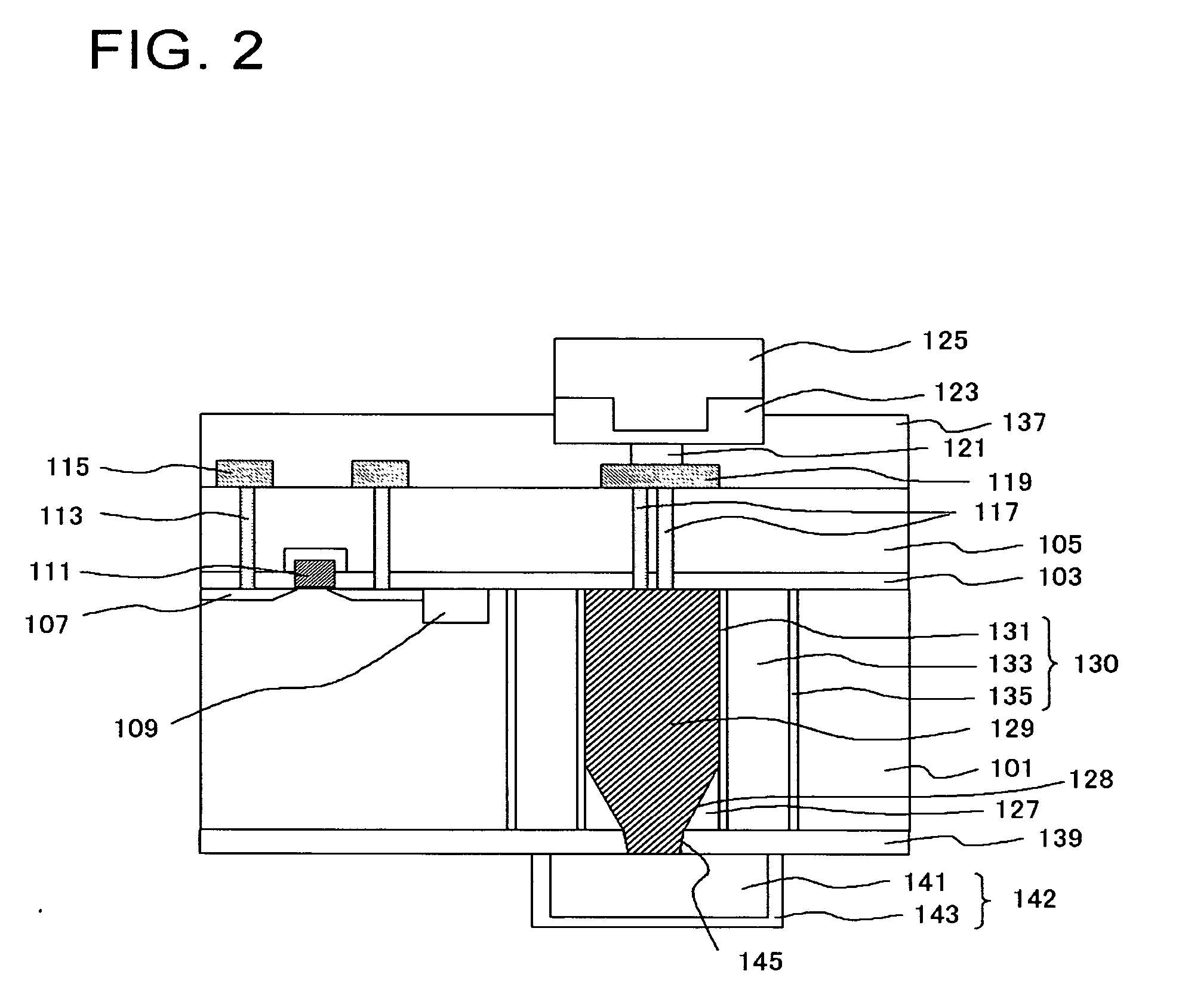
[0116]FIG. 3 is a cross-sectional view, illustrating a configuration of a semiconductor device of the present embodiment. Fundamental configuration of the semiconductor device shown in FIG. 3 is similar to the semiconductor device 100 illustrated in FIG. 1, except that a silicon substrate remaining portion 149 is provided to surround and covers the entire inner surface of the first insulating ring 130. The silicon substrate remaining portion 149 is an annular region, having a geometry, in which an inner diameter thereof is increased from the device-forming surface toward the interior of the silicon substrate 101 in the vicinity of the device-forming surface of the silicon substrate 101, and an inner diameter thereof is increased from the back surface toward the interior of the silicon substrate 101 in the vicinity of the back surface.

[0117] Since the protruding portion is also provided at least in the vicinity of the device-forming surface and the back surface of the silicon substr...


PUM


Abstract

A falling off of a through electrode is inhibited without decreasing a reliability of a semiconductor device including a through electrode. A semiconductor device 100 includes: a silicon substrate 101; a through electrode 129 extending through the silicon substrate 101; and a first insulating ring 130 provided in a circumference of a side surface of the through electrode 129 and extending through the semiconductor substrate 101. In addition, the semiconductor device 100 also includes a protruding portion 146, being provided at least in the vicinity of a back surface of a device-forming surface of the semiconductor substrate 101 so as to contact with the through electrode 129, and protruding in a direction along the surface of the semiconductor substrate 101 toward an interior of the through electrode 129.

Description

[0001] This application is based on Japanese patent application No. 2005-284,248, the content of which is incorporated hereinto by reference. BACKGROUND [0002] 1. Technical Field [0003] The present invention relates to a semiconductor device and a method for manufacturing thereof. [0004] 2. Related Art [0005] In recent years, lighter, more compact and more sophisticated semiconductor devices are generally required in the industry, a dense installation of interconnects, a miniaturization of a logical device and an increased capacity of a memory are proceeded in semiconductor devices such as a multi-chip package. [0006] A solution for such requirements is an attempt for achieving a dense installation of interconnects by providing a through electrode in a semiconductor substrate. Typical conventional through electrode is described in Japanese Patent Laid-Open No. S60-140,850 (1985). A device is described in Japanese Patent Laid-Open No. S60-140,850, in which an aperture is provided in ...

Claims


Application Information

Patent Timeline
IPC IPC(8): H01L21/20
CPCH01L21/76898H01L23/481H01L2224/14181H01L2224/13025H01L2224/13H01L23/485
Inventor KAWANO, MASAYASOEJIMA, KOJITAKAHASHI, NOBUAKI
Owner RENESAS ELECTRONICS CORP
Why Eureka
Try Eureka