Chip package and method of fabricating the same

Inactive Publication Date: 2008-09-18
CHIPMOS TECH INC
View PDF3 Cites 8 Cited by
  • Summary
  • Abstract
  • Description
  • Claims
  • Application Information

AI Technical Summary

Benefits of technology

[0011]Accordingly, the present invention is directed to a chip package and a method of fabricating the same for resolving the problem of high cost when a patterned lead frame is directly used. The present inventi

Problems solved by technology

Because expensive exposure and development masks are required to patter

Method used


Image

  • Chip package and method of fabricating the same
  • Chip package and method of fabricating the same
  • Chip package and method of fabricating the same

Examples


Embodiment Construction

[0025]Reference will now be made in detail to the present preferred embodiments of the invention, examples of which are illustrated in the accompanying drawings. Wherever possible, the same reference numbers are used in the drawings and the description to refer to the same or like parts.

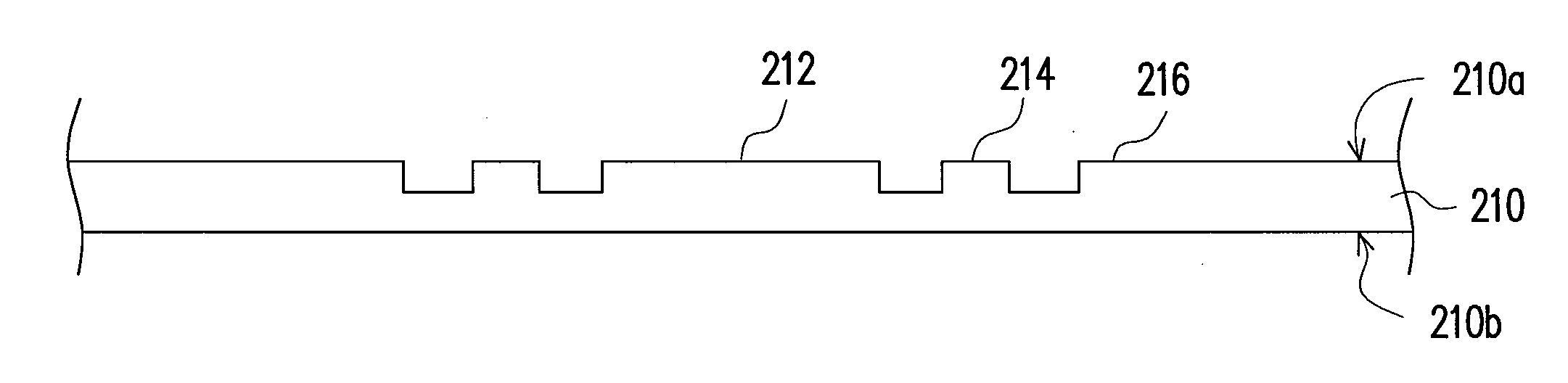
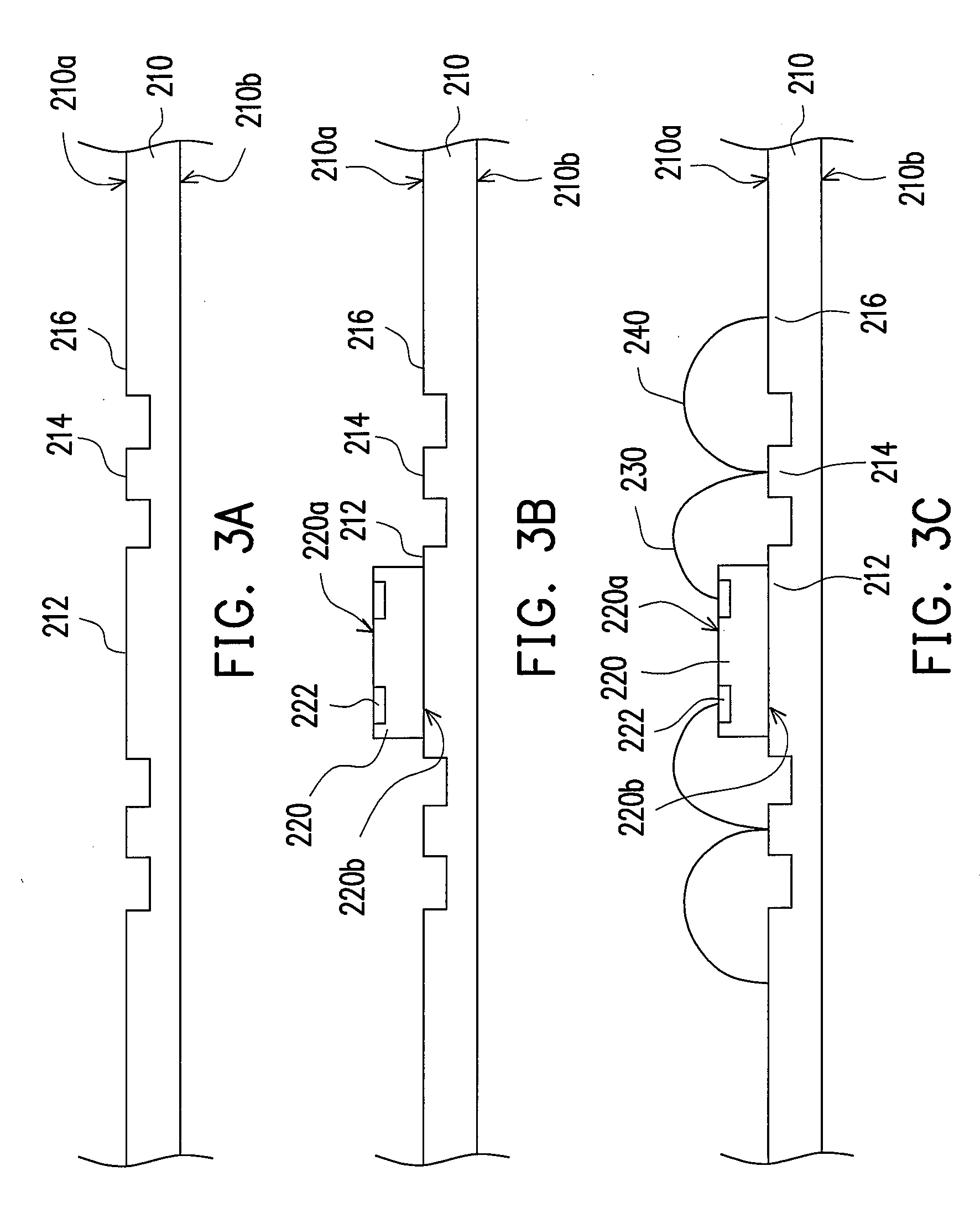
[0026]FIGS. 3A to 3F are schematic cross-sectional views illustrating the process for fabricating a chip package according to an embodiment of the present invention. First, as shown in FIG. 3A, a thin metal plate 210 is provided. The thin metal plate 210 has an upper surface 210a and a lower surface 210b. The upper surface 210a has a plurality of trenches so as to divide the thin metal plate 210 into a first protrusion part 212, a second protrusion part 214 and a plurality of third protrusion parts 216. Furthermore, the first protrusion part 212, the second protrusion part 214 and the third protrusion parts 216 are connected to one another. The first protrusion part 212 is substantially located in th...


PUM


Abstract

A method of fabricating a chip package is provided. A thin metal plate having a first protrusion part, a second protrusion part and a plurality of third protrusion parts are provided. A chip is disposed on the thin metal plate, and a plurality of bonding wires for electrically connecting the chip to the second protrusion part and the second protrusion part to the third protrusion parts is formed. An upper encapsulant and a lower encapsulant are formed on the upper surface and the lower surface of the thin metal plate respectively. The lower encapsulant has a plurality of recesses for exposing a portion of the thin metal plate at locations where the first protrusion part, the second protrusion part and the third protrusion parts are connected to one another. Finally, the thin metal plate is etched by using the lower encapsulant as an etching mask.

Description

CROSS-REFERENCE TO RELATED APPLICATION[0001]This application claims the priority benefit of P.R.C. application serial no. 200710087671.6, filed Mar. 13, 2007. All disclosure of the P.R.C. application is incorporated herein by reference.BACKGROUND OF THE INVENTION[0002]1. Field of the Invention[0003]The present invention generally relates to a chip package, in particular, to a chip package having a lead frame.[0004]2. Description of Related Art[0005]In the semiconductor industry, the fabrication of integrated circuits (IC) can be divided into three major stages: IC design stage, IC process stage and IC package stage.[0006]In the fabrication of IC, the steps of producing a chip include at least wafer fabrication, IC formation and wafer sawing. The wafer has an active surface, in which active elements are formed. After the fabrication of IC in the wafer is completed, a plurality of bonding pads is disposed on the active surface of the wafer so that the chip subsequently cut out from th...

Claims


Application Information

Patent Timeline
IPC IPC(8): H01L23/495
CPCH01L21/4832H01L23/3107H01L2924/01033H01L2924/01006H01L24/48H01L2924/19107H01L23/49541H01L24/49H01L2221/68377H01L2224/48091H01L2224/48247H01L2224/4911H01L2924/01005H01L2924/01015H01L2924/01029H01L2924/01082H01L2924/14H01L2924/00014H01L2924/181H01L2224/05554H01L2924/10161H01L2224/45099H01L2224/05599H01L2924/00012
Inventor QIAO, YONG-CHAOCHIOU, JIE-HUNGWU, YAN-YI
Owner CHIPMOS TECH INC
Why Eureka
Try Eureka