Light-emitting device, image forming apparatus, display device, and electronic apparatus

a technology of light-emitting devices and display devices, which is applied in the direction of organic semiconductor devices, electroluminescent light sources, electric lighting sources, etc., can solve the problems of top-emission-type light-emitting devices, large damage to light-emitting layers, and application of techniques

Active Publication Date: 2007-12-20
SEIKO EPSON CORP
View PDF14 Cites 23 Cited by
  • Summary
  • Abstract
  • Description
  • Claims
  • Application Information

AI Technical Summary

Problems solved by technology

However, in the case of the top-emission-type light-emitting device to which the technique disclosed in Japanese Patent No. 3274527 is applied, it is necessary to form a dielectric mirror on EL elements formed on a substrate in manufacturing the top-emission-type light-emitting device, which may cause the EL elements (for example, light-emitting layer) to be greatly damaged.
Since the light emission characteristics of the EL elements that are greatly damaged noticeably deteriorate, it is difficult to apply the technique disclosed in Japanese Patent No. 3274527 to the top-emission-type light-emitting device.

Method used


Image

  • Light-emitting device, image forming apparatus, display device, and electronic apparatus
  • Light-emitting device, image forming apparatus, display device, and electronic apparatus
  • Light-emitting device, image forming apparatus, display device, and electronic apparatus

Examples


first embodiment

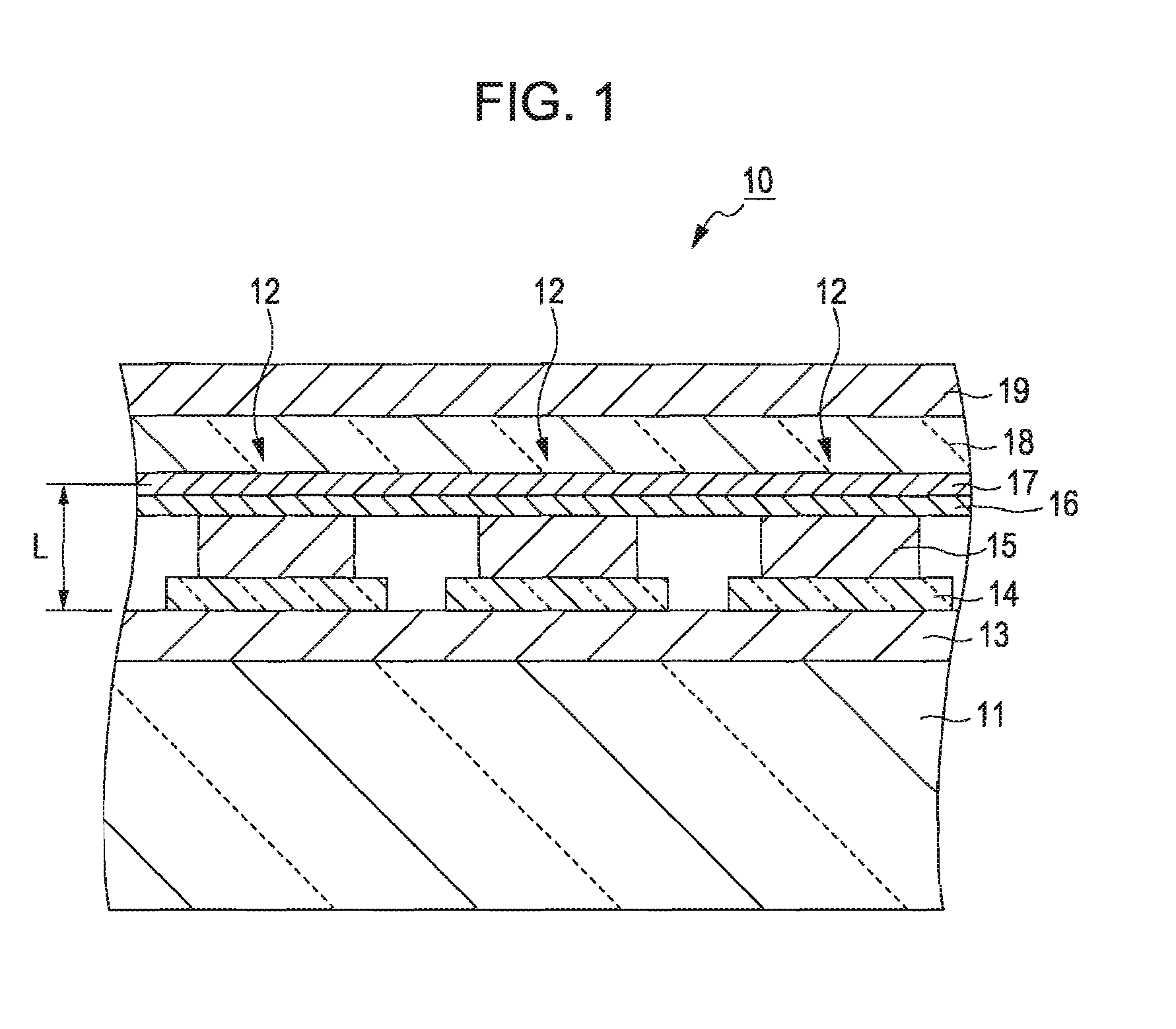
[0079]FIG. 1 is a cross-sectional view illustrating a part of a light-emitting device 10 according to a first embodiment of the invention. The light-emitting device 10 has a plurality of light-emitting elements 12 arranged on a substrate 11. In FIG. 1, only three light-emitting elements 12 are shown. Each of the light-emitting elements 12 is an organic EL element, that is, an OLED (organic light-emitting diode) element. That is, the light-emitting device 10 is an organic EL device.

[0080]The substrate 11 is formed of a glass, for example, and the thickness of the substrate 11 is 500 μm, for example. On the substrate 11, a light reflection layer 13 from which light is totally reflected is formed. The light reflection layer 13 allows light to resonate and is formed of a material having a high optical reflectance. In addition, an upper surface of the light reflection layer 13 is smooth and the thickness of the light reflection layer 13 is 200 nm, for example. Specifically, the material ...

second embodiment

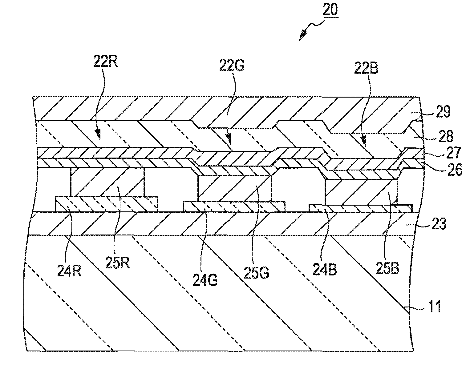
[0101]FIG. 14 is a cross-sectional view illustrating a part of a light-emitting device 20 according to a second embodiment of the invention. The second embodiment is different from the first embodiment in that a full color image can be displayed. The light-emitting device 20 is suitable for display of a full color image and has a plurality of pixels arranged in a matrix on a light reflection layer 23. Each of the pixels includes a light-emitting element 22R that emits ‘R’ light corresponding to a color close to a red color, a light-emitting element 22G that emits ‘G’ light corresponding to a color close to a green color, and a light-emitting element 22B that emits ‘B’ light corresponding to a color close to a blue color. Although the light emitting elements 22R, 22G, and 22B are described as emitting red color, green color, and blue color, respectively, it should be noted that elements that emit light near to these colors could be used instead.

[0102]The configuration below the light...

third embodiment

[0115]FIG. 23 is a cross-sectional view illustrating a part of a light-emitting device 50 according to a third embodiment of the invention. The third embodiment is different from the first embodiment in that a transparent layer is provided between the light reflection layer 13 and the transparent electrodes 14. The light-emitting device 50 has a plurality of light-emitting elements 52 arranged on a substrate 51. In FIG. 23, only three light-emitting elements 52 are shown. Each of the light-emitting elements 52 is an organic EL element, that is, an OLED (organic light-emitting diode) element. That is, the light-emitting device 50 is an organic EL device.

[0116]The substrate 51 is formed of a glass, for example, and the thickness of the substrate 51 is 500 μm, for example. On the substrate 51, a light reflection layer 53 from which light is totally reflected is formed. The light reflection layer 53 allows light to resonate and is formed of a material having a high optical reflectance. ...


PUM


Abstract

A light-emitting device includes: a substrate; a light reflection layer that is formed on the substrate and reflects light; a first electrode that is formed on the light reflection layer and transmits light; a light-emitting layer that is formed on the first electrode and emits light; a second electrode that is formed on the light-emitting layer and transmits a part of light from the light-emitting layer and reflects the rest of the light from the light-emitting layer; and a conductive transflective layer that is formed on the second electrode and that transmits a part of light from the second electrode and reflects the rest of the light from the second electrode. A work function of the second electrode is 4 eV (electron volts) or less. The conductive transflective layer is formed of a metal material having a higher optical reflectance than the second electrode.

Description

BACKGROUND[0001]1. Technical Field[0002]The present invention relates to a light-emitting device, an image forming apparatus, a display device, and an electronic apparatus.[0003]2. Related Art[0004]In a light-emitting device having EL (electroluminescent) elements, such as organic EL elements or inorganic EL elements, it is necessary to make a band of an emission spectrum narrow and to increase an amount of emitted light for the purpose of facilitating many applications thereof. As a light-emitting device that meets the above requirements, there is a light-emitting device having microcavities formed by arranging a dielectric mirror between EL elements and a substrate (refer to Japanese Patent No. 3274527). The light-emitting device is of a bottom emission type, and light from EL elements is transmitted through the substrate and is then emitted.[0005]In a light-emitting device having EL elements, a substrate on which the EL elements are arranged is very thick. Therefore, from the poi...

Claims


Application Information

Patent Timeline
Patent Type & Authority Applications(United States)
IPC IPC(8): H01L33/00
CPCH01L27/3211H01L2251/5315H01L51/5265H10K59/351H10K50/852H10K2102/3026H05B33/26H05B33/28
Inventor KOBAYASHI, HIDEKAZU
Owner SEIKO EPSON CORP
Why Eureka
Try Eureka