Semiconductor device and electronic device

a technology of semiconductor devices and electronic devices, applied in semiconductor devices, digital storage, instruments, etc., can solve the problems of increasing power consumption involved in data reading, and power consumption has been particularly high, and achieves the effect of low power consumption memory

Inactive Publication Date: 2008-01-03
SEMICON ENERGY LAB CO LTD
View PDF9 Cites 27 Cited by
  • Summary
  • Abstract
  • Description
  • Claims
  • Application Information

AI Technical Summary

Benefits of technology

[0059]In accordance with the present invention, regarding a semiconductor device mounted with a memory, bit lines can be selectively precharged. In other words, bit lines which are not associated with reading of data from a memory are not precharged; thus, a semiconductor device having a low power consumption memory can be obtained.

Problems solved by technology

As to semiconductor devices mounted with memories, increase in power consumption involved in reading of data has become significant associated with increase in memory capacity in recent years.
Accordingly, when data of ROM is read, power consumption has particularly increased significantly.

Method used


Image

  • Semiconductor device and electronic device
  • Semiconductor device and electronic device
  • Semiconductor device and electronic device

Examples


embodiment mode 1

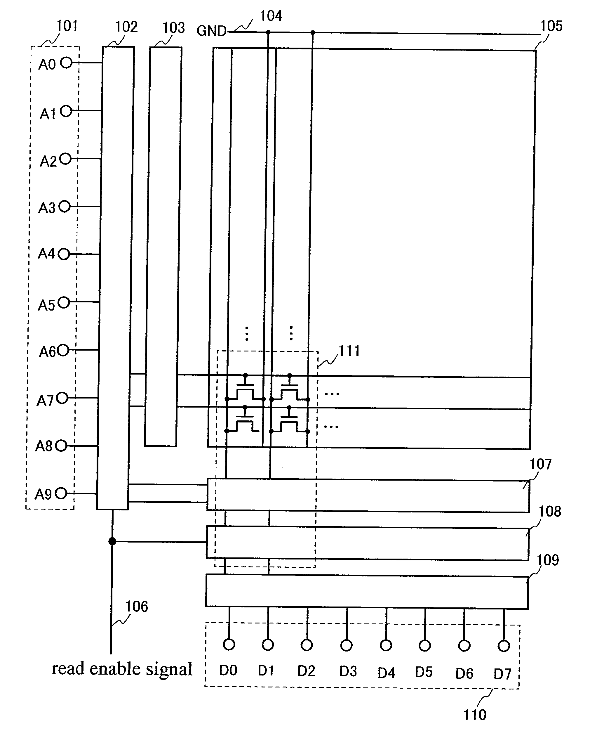
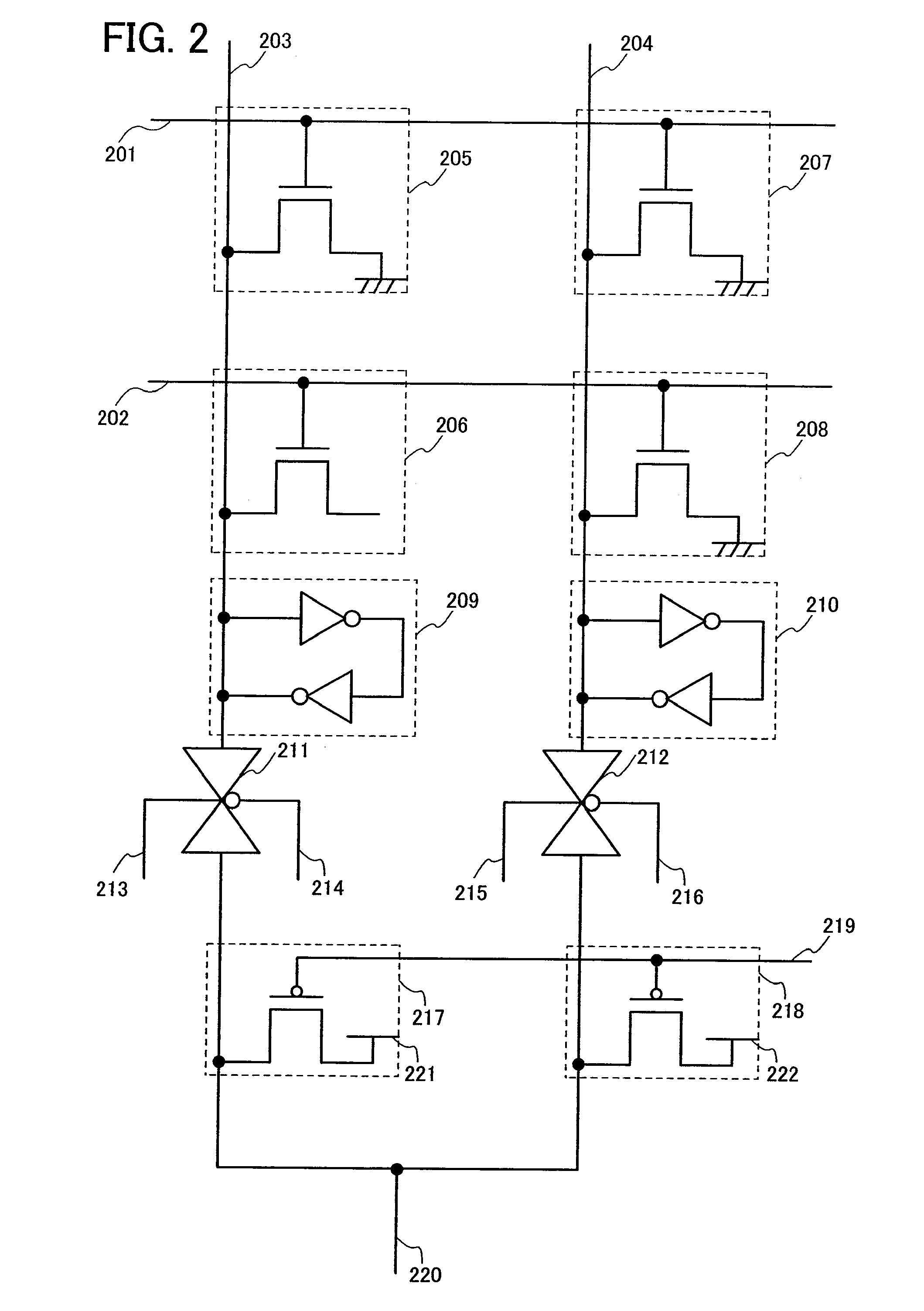
[0082]This embodiment mode will be described with reference to FIG. 1, FIG. 2, and FIG. 3. FIG. 1 is a block diagram of a mask ROM of the present invention. Further, FIG. 2 is a circuit diagram of the invention, in which a region 111 in FIG. 1 is enlarged. Further, FIG. 3 is a timing chart of the circuit diagram shown in FIG. 2. Note that in this embodiment mode, a memory having memory cells of two rows and two columns will be described; however, n rows and m columns can be generally used (n and m are natural numbers).

[0083]In this embodiment mode, a ROM where data is read will be described using a mask ROM as an example. In FIG. 1, the mask ROM includes address signal lines 101, an address input buffer 102, a row decoder 103, a ground line 104, a memory matrix 105, a read enable signal line 106, a switching circuit 107, a precharge circuit 108, a data output buffer 109, and data signal lines 110.

[0084]In FIG. 1, explanation will be made assuming that the address signal lines 501 in...

embodiment mode 2

[0112]In this embodiment mode, a structure different from the structure described in the above Embodiment Mode 1 will be explained.

[0113]Note that a block diagram of the structure of a mask ROM of this embodiment mode is similar to the structure described in Embodiment Mode 1 with reference to FIG. 1. Therefore, in this embodiment mode, the description is to be referred to the description of FIG. 1 explained in Embodiment Mode 1.

[0114]Further, FIG. 4 is a circuit diagram of a mask ROM of this embodiment mode. In this embodiment mode, the region 111 in FIG. 1, explained in Embodiment Mode 1 includes an n-th word line 201, an (n+1)th word line 202, an m-th bit line 203, an (m+1)th bit line 204, a memory cell 205 of n-th row and m-th column, which is arranged at the point where the n-th word line 201 and the m-th bit line 203 intersect, a memory cell 206 of (n+1)th row and m-th column, which is arranged at the point where the (n+1)th word line 202 and the m-th bit line 203 intersect, a...

embodiment 1

[0122]A memory of the present invention can be used for electronic appliances of a variety of fields that are equipped with a memory. That is, the present invention includes electronic appliances equipped with a memory. For example, a camera such as a video camera or a digital camera; a goggle-type display (head-mounted display); a navigation system; a sound reproduction system (a car audio system, an audio component, and the like); a computer; a game machine; a portable information terminal (a mobile computer, a portable phone, a portable game machine, an electronic book, and the like); an image reproduction device equipped with a recording medium (specifically, a device that can reproduce a recording medium such as a DVD (digital versatile disc) and that is equipped with a display that can display the image); and the like can be given as electronic appliances to which the semiconductor device of the present invention is applied. Specific examples of such electronic appliances are ...


PUM


Abstract

In relation to reading of data in a memory, it is an object to provide a semiconductor device mounted with a low power consumption memory. A semiconductor device including a word line, a bit line, and a memory cell electrically connected to the word line and the bit line, further includes a precharge circuit for making the bit line have an electric potential for reading data stored in the memory cell. The precharge circuit is provided for each bit line and connected to the bit line. Further, the precharge circuit is capable of making each bit line have an electric potential for reading the data stored in the memory cell for each bit line.

Description

BACKGROUND OF THE INVENTION[0001]1. Field of the Invention[0002]The present invention relates to semiconductor devices. In particular, the present invention relates to semiconductor devices each mounted with a memory. Further, the present invention relates to electronic devices mounted with the semiconductor devices[0003]2. Description of the Related Art[0004]Regarding a semiconductor device mounted with a memory, the performance of the memory is extremely important because the performance of the semiconductor device depends on it. For example, as to a semiconductor device mounted with a CPU and a memory, commands to be processed by the CPU and data necessary for the processing need to be stored in the memory. Further, processing by the CPU is progressed by sequential reading of the data in the memory. In other words, as to a semiconductor device mounted with a CPU and a memory, in order to achieve higher performance, the CPU needs to be able to handle more complicated processes, an...

Claims


Application Information

Patent Timeline
Patent Type & Authority Applications(United States)
IPC IPC(8): G11C11/40
CPCG11C7/12H01L27/12H01L27/112H01L21/84H10B20/00G11C11/4074G11C11/40
Inventor INOUE, TAKAYUKIKUROKAWA, YOSHIYUKIIKEDA, TAKAYUKI
Owner SEMICON ENERGY LAB CO LTD
Why Eureka
Try Eureka