Alignment and cutting of microelectronic substrates

a technology of microelectronic substrates and cutting holes, which is applied in the direction of printed circuits, solid-state devices, printed circuit manufacturing, etc., can solve the problems of inaccuracy in the offset between the package pin and the outer periphery of the chip carrier, and the placement of holes on the substrate can be imprecise or misaligned

Inactive Publication Date: 2008-07-03
TESSERA INC
View PDF8 Cites 119 Cited by
  • Summary
  • Abstract
  • Description
  • Claims
  • Application Information

AI Technical Summary

Problems solved by technology

However, the above alignment of the substrate relative to the frame has the disadvantage that the position of holes on the substrate can be imprecise or misaligned relative to the position of the package pins.
This can lead to inaccuracy in the offset between the package pins and the outer periphery of the chip carriers.

Method used


Image

  • Alignment and cutting of microelectronic substrates
  • Alignment and cutting of microelectronic substrates
  • Alignment and cutting of microelectronic substrates

Examples


Embodiment Construction

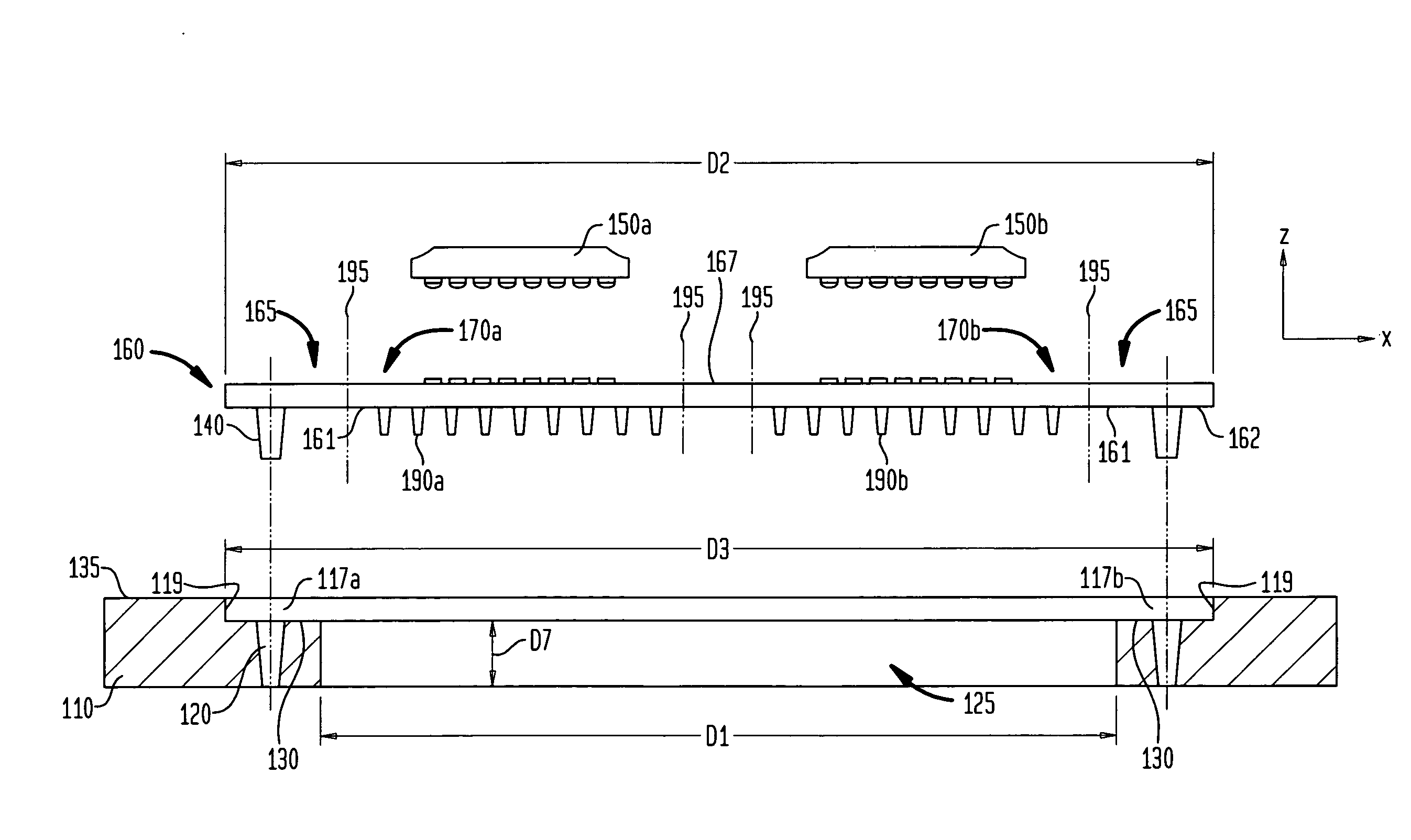
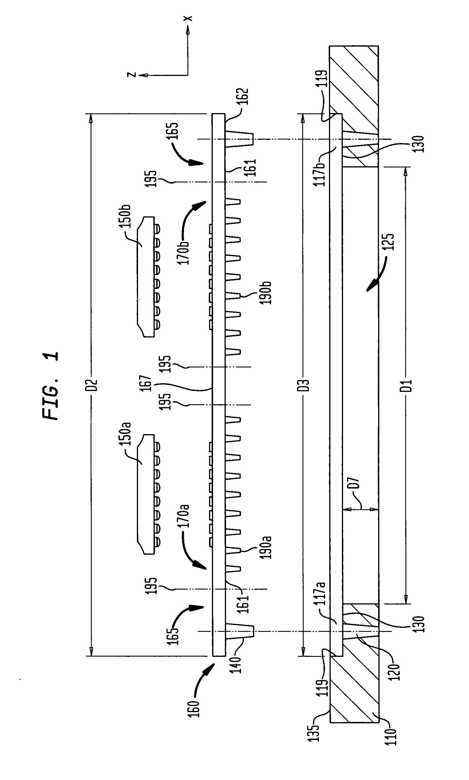
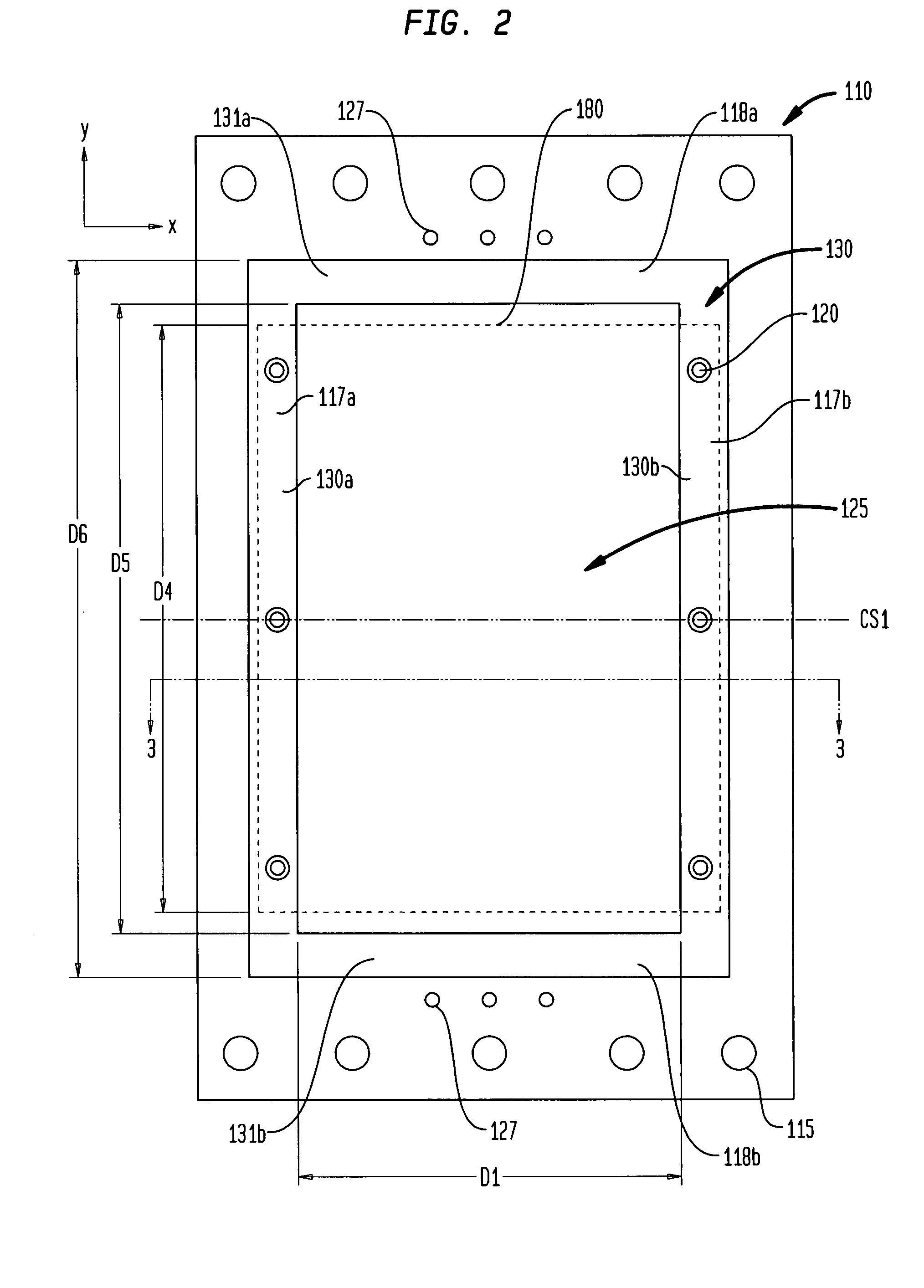
[0020]FIG. 1 schematically depicts a cross-sectional view of a stage of a method according to a first embodiment of the present invention. The cutting line CS1 of the cross-sectional view that is shown in FIG. 1 is indicated in FIG. 2. FIG. 1 shows an in-process element of a microelectronic device packaging and processing method, being a substrate or tape 160 that is to be mated and aligned with a frame 110. With reference to FIG. 1, an X-direction points to the right in parallel to the substrate 160, the Y-axis points away from the perspective of the viewer, while the Z-axis is indicated and points towards the top of FIG. 1. As used in this disclosure, terms such as “upwardly,”“upper,”“top,”“downwardly,”“lower,”“bottom,”“vertically,” and “horizontally” should be understood as referring to the frame of reference of the element specified, and need not conform to the normal gravitation frame of reference.

[0021]Frame 110 has an opening 125 with length D5 (FIG. 2) and width D1, that is ...


PUM

PropertyMeasurementUnit
diameteraaaaaaaaaa
metallicaaaaaaaaaa
areasaaaaaaaaaa

Abstract

A substrate including plural microelectronic device carriers has metallic alignment elements. The alignment elements desirably are disposed in a predetermined positional relationship to terminals on the carriers. The alignment elements are engaged with a carrier frame and a cutting device is aligned with the carrier frame. The cutting device cuts the carriers so that borders of the carriers are in a precise relationship with the terminals.

Description

FIELD OF THE INVENTION[0001]The present invention relates to the cutting of individual chip carriers from a tape or substrate that is configured to hold a plurality of microelectronic devices.BACKGROUND OF THE INVENTION[0002]In conventional methods for cutting out individual chip carriers from a tape or substrate having multiple chip carriers that have been manufactured commonly in a previous step, a substrate for holding multiple chips can be put into a punch index frame. The punch index frame is typically a rectangular frame with a rectangular opening in the middle configured to hold the substrate in the frame at a fixed position. The punch index frame can be positioned in X- and Y-directions parallel to the plane of the substrate by linear motion relative to a cutting tool. For positioning of the substrate in relation to the punch index frame, to guarantee that the substrate is cut at the right position, alignment holes are arranged on the punch index frame and on the substrate i...

Claims


Application Information

Patent Timeline
Patent Type & Authority Applications(United States)
IPC IPC(8): H05K13/00H01S4/00H05K1/00
CPCH01L24/16Y10T29/49002H01L24/48H01L24/97H01L2224/16225H01L2224/32225H01L2224/48091H01L2224/48227H01L2224/73265H01L2224/97H01L2924/01082H01L2924/078H01L2924/10156H01L2924/10158H01L2924/19107H05K3/0052H05K2203/0165H05K2203/0228H05K2203/167H01L24/32Y10T29/49169H01L2924/01033H01L2924/01023H01L2924/00014H01L2224/81H01L2224/83H01L2224/85H01L2924/00H01L2224/0554H01L2224/05568H01L2224/05573H01L2224/05599H01L2224/45099H01L2224/45015H01L2924/207H01L2224/0555H01L2224/0556
Inventor HONER, KENNETH ALLENWADE, CHRISTOPHER PAULTOBE, SEIICHITSENG, CHUNG-CHUANCHAU, ELLISBANG, KYONG-MO
Owner TESSERA INC
Why Eureka
Try Eureka