Electrostatic discharge protection circuit having multiple discharge paths

a protection circuit and electrostatic discharge technology, applied in the direction of semiconductor devices, semiconductor/solid-state device details, transistors, etc., can solve the problems of insufficient protection of internal circuits, decrease in gate oxide thickness, and decrease in technology size, so as to enhance electrostatic discharge performance and enhance electrostatic discharge speed

Inactive Publication Date: 2008-08-21
SK HYNIX INC
View PDF10 Cites 17 Cited by
  • Summary
  • Abstract
  • Description
  • Claims
  • Application Information

AI Technical Summary

Benefits of technology

[0016]The present invention provides an electrostatic discharge protection circuit in which a driving voltage of the electrostatic discharge protection circuit is lowered to enhance an electrostatic discharge speed.
[0017]Further present invention provides an electrostatic discharge protection circuit in which a resistance of a driving line providing a driving voltage of an electrostatic discharge protection device is properly controlled to enhance an electrostatic discharge performance.

Problems solved by technology

However, in the conventional electrostatic discharge protection circuit, which uses only the parasitic bipolar operation as shown in FIG. 1, problems arise as a result of decreasing size of the technology, for example decrease in a gate oxide thickness.
The conventional electrostatic discharge protection circuit as shown in FIG. 1 cannot sufficiently protect the internal circuit 14 due to its limitation in operation speed.
However, since the total series resistance of the resistor R3, the capacitor C3, and the resistor R4 is large, it is difficult for static current to flow in a gate of the respective MOS transistors P3, N4, and N5; and as a result electrostatic discharge performance may be diminished.

Method used


Image

  • Electrostatic discharge protection circuit having multiple discharge paths
  • Electrostatic discharge protection circuit having multiple discharge paths
  • Electrostatic discharge protection circuit having multiple discharge paths

Examples


Embodiment Construction

[0042]Hereinafter, preferred embodiments of the present invention will be described in detail with reference to the accompanying drawings.

[0043]In an electrostatic discharge protection circuit of the present invention, a trigger circuit using a gate coupled MOS (GCMOS) transistor is coupled to the gate of a main electrostatic discharge protection device to apply a bias, thereby lowering the operation voltage of the main electrostatic discharge protection device.

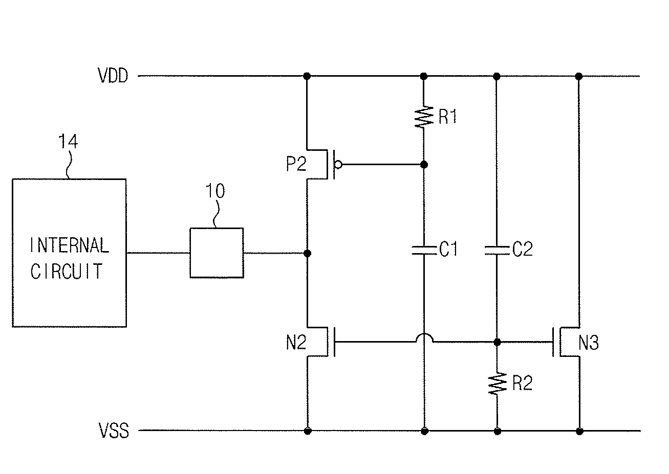
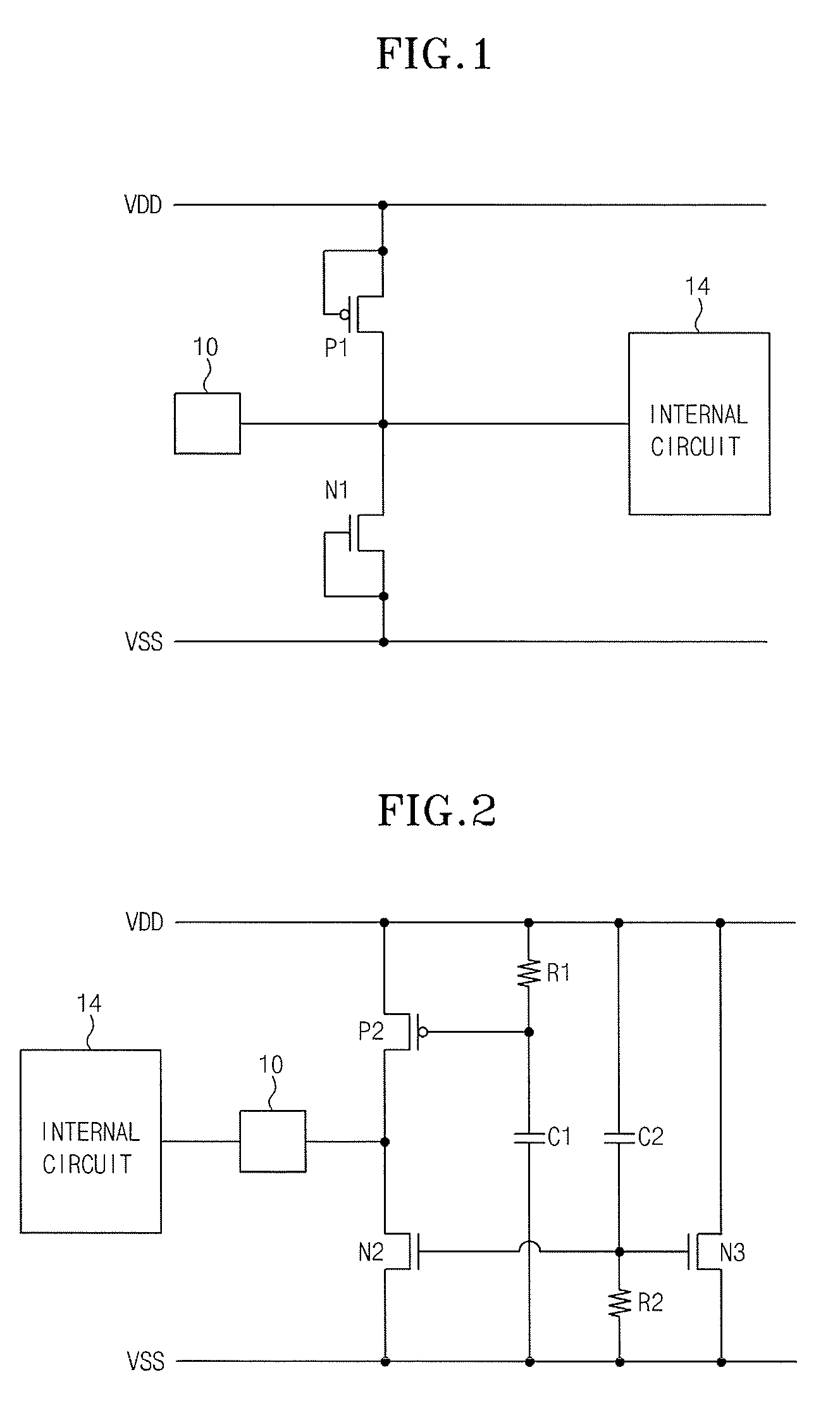
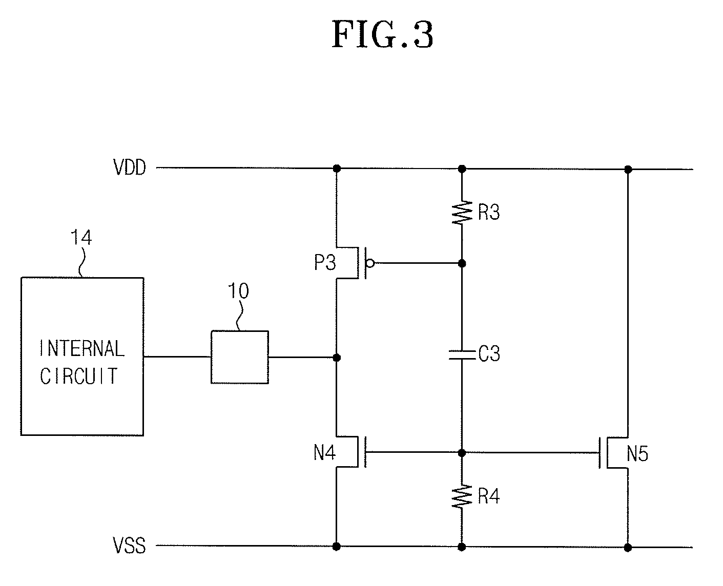
[0044]Specifically, referring to FIG. 4, an electrostatic discharge protection circuit of the present invention includes a trigger unit 40, a trigger unit 42, and an electrostatic discharge protection unit 44.

[0045]The trigger unit 40 provides a trigger voltage VTRIG1 to a node NODE13 A in response to static electricity transferred from at least one of a power voltage line VDD and a ground voltage line VSS. For example, a potential drop occurs when static electricity is transferred from at least one of a power voltage line VD...


PUM


Abstract

The present invention relates to an electrostatic discharge protection circuit of a semiconductor memory device to protect an internal circuit from static electricity. The electrostatic discharge protection circuit includes a first trigger unit which provides a first trigger voltage in response to static electricity transferred from at least one of a first and second voltage line. A second trigger unit provides a second trigger voltage by the static electricity in response to the first trigger voltage. An electrostatic discharge protection unit configures an electrostatic discharge path among the first voltage line, the second voltage line and an input/output pad in response the first and second trigger voltages. The electrostatic discharge speed of the electrostatic discharge protection unit is enhanced by the first and second trigger voltages.

Description

CROSS-REFERENCE TO RELATED APPLICATIONS[0001]The present application claims priority to Korean patent application number 10-2007-0016263 filed on Feb. 15, 2007, which is incorporated herein by reference in its entirety.BACKGROUND OF THE INVENTION[0002]The present invention relates generally to an electrostatic discharge protection circuit, and more particularly to an electrostatic discharge protection circuit of a semiconductor memory device to protect an internal circuit from static electricity.[0003]In general, a MOS transistor is one of the devices typically used as an electrostatic discharge protection circuit. FIG. 1 shows a widely used structure for an electrostatic discharge protection circuit, where a PMOS transistor Pt is coupled between a power voltage line VDD and an input / output pad 10 and an NMOS transistor N1 is coupled between a ground voltage line VSS and the input / output pad 10.[0004]As shown in FIG. 1, the gate of the NMOS transistor N1 and the gate of the PMOS tra...

Claims


Application Information

Patent Timeline
Patent Type & Authority Applications(United States)
IPC IPC(8): H01L23/62H02H9/00
CPCH02H9/046H01L27/0266H01L23/60H01L27/04
Inventor YUN, SUK
Owner SK HYNIX INC
Why Eureka
Try Eureka