3-Dimensional Device Design Layout

a three-dimensional device and design layout technology, applied in the field of semiconductor devices, can solve the problems of inability of the gate to substantially control the on and off, the short gate length of the transistor, and the need for considerable time for designing and laying out the circuit of three-dimensional devices

Active Publication Date: 2008-10-23
TAIWAN SEMICON MFG CO LTD
View PDF24 Cites 112 Cited by
  • Summary
  • Abstract
  • Description
  • Claims
  • Application Information

AI Technical Summary

Benefits of technology

[0007]These and other problems are generally solved or circumvented, and technical advantages are generally achieved, by preferred e...

Problems solved by technology

Consequently, a transistor with a short gate length suffers from problems related to the inability of the gate to substantially control the on and off states of the channel.
However, the three-dimensional devices may requi...

Method used


Image

  • 3-Dimensional Device Design Layout
  • 3-Dimensional Device Design Layout
  • 3-Dimensional Device Design Layout

Examples


Embodiment Construction

[0018]The making and using of the presently preferred embodiments are discussed in detail below. It should be appreciated, however, that the present invention provides many applicable inventive concepts that can be embodied in a wide variety of specific contexts. The specific embodiments discussed are merely illustrative of specific ways to make and use the invention, and do not limit the scope of the invention.

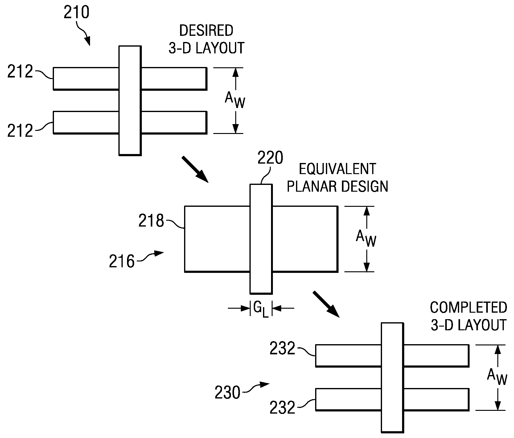
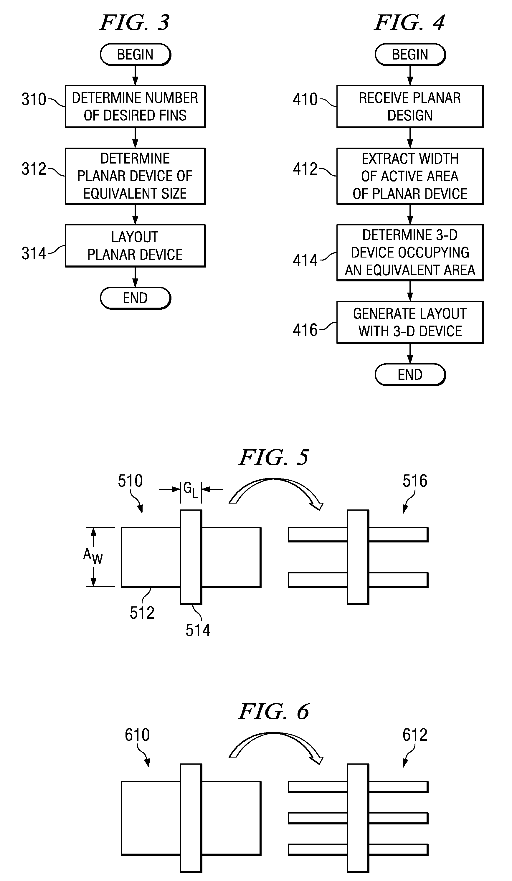
[0019]The present invention will be described with respect to preferred embodiments in a specific context, namely a layout design including a finFET. The invention may also be applied, however, to other 3-dimensional devices, including raised fuses, resistors, and the like.

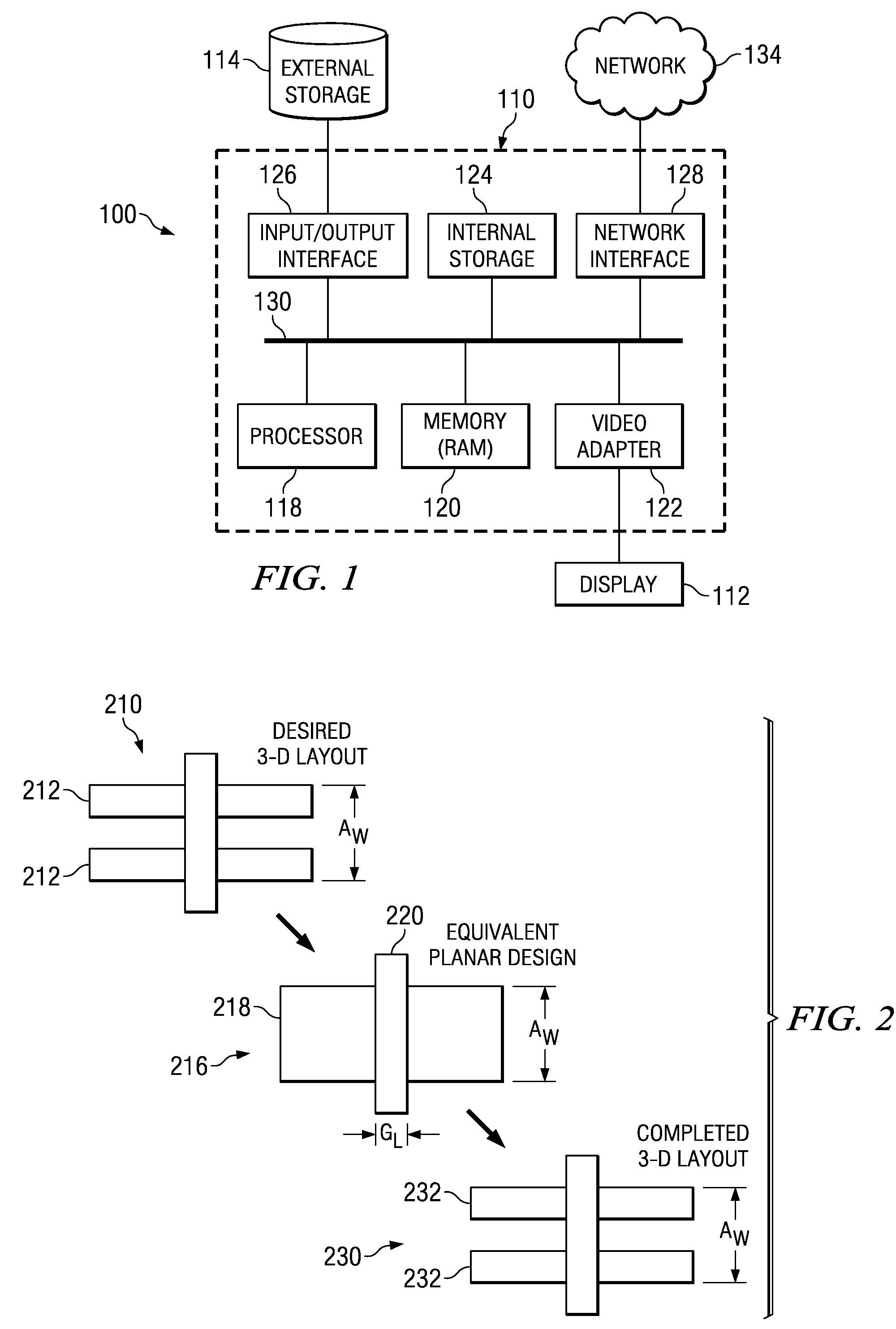
[0020]It is further noted that, unless indicated otherwise, all functions described herein may be performed in either hardware or software, or some combination thereof. In a preferred embodiment, however, the functions are performed by a processor such as a computer or an electronic data processor in accord...


PUM


Abstract

A method for defining a layout of 3-D devices, such as a finFET, is provided. The method includes determining an area required by a desired 3-D device and designing a circuit using planar devices having an equivalent area. The planar device corresponding to the desired 3-D device is used to layout a circuit design, thereby allowing circuit and layout designers to work at a higher level without the need to specify each individual fin or 3-D structure. Thereafter, the planar design may be converted to a 3-D design by replacing planar active areas with 3-D devices occupying an equivalent area.

Description

[0001]This application claims the benefit of U.S. Provisional Application No. 60 / 925,046, filed on Apr. 18, 2007, entitled “3-Dimensional Device Design Layout,” which application is hereby incorporated herein by reference.TECHNICAL FIELD[0002]The present invention relates generally to semiconductors and, more particularly, to a system and method for specifying a design layout for three-dimensional devices.BACKGROUND[0003]Traditional semiconductor devices utilized planar devices in which portions of a substrate are doped to create a conductive region. This technology has been used in manufacturing ultra-large scale integrated (ULSI) circuits incorporating metal-oxide-semiconductor field effect transistors (MOSFETs). Reduction in the size of MOSFETs has provided continued improvement in speed, performance, circuit density, and cost per unit function over the past few decades. As the gate length of the conventional bulk MOSFET is reduced, the source and drain increasingly interact with...

Claims


Application Information

Patent Timeline
IPC IPC(8): G06F17/50
CPCH01L21/76807H01L21/76895H01L21/76897H01L21/823431H01L21/823437H01L21/823475H01L29/41791H01L29/66795H01L29/785H01L2029/7858
Inventor CHUANG, HARRYTHEI, KONG-BENGLIANG, MONG SONGCHUNG, SHENG-CHENYAO, CHIH-TSUNGKAO, JUNG-HUICHENG, CHUNG LONGSHEN, GARYCHANG, GWAN SIN
Owner TAIWAN SEMICON MFG CO LTD
Why Eureka
Try Eureka