Fingerprint Sensing Circuit

a fingerprint sensing and circuit technology, applied in the field can solve the problems of high circuit implementation cost, limited application of fingerprint sensing circuits, and inability to work well with optical-based recognition methods, etc., and achieves the effects of less power consumption, improved sensing results, and easy implementation

Active Publication Date: 2008-12-25
XUESHAN TECH INC
View PDF5 Cites 18 Cited by
  • Summary
  • Abstract
  • Description
  • Claims
  • Application Information

AI Technical Summary

Benefits of technology

[0006]The fingerprint sensing circuit is less constrained by the frequency of the signal source, and the AD converter does not process high frequency AC analog signals related to the signal source because the AD converter now processes DC analog signals. In summary, the fingerprint sensing circuit of the present invention can yield m

Problems solved by technology

However, optical-based recognition methods may not work well if optical sensing devices are defaced and damaged, and may also be cheated by using pictures or patterns which have correct fingerprints thereon.
Thus, to cover an extended application ra

Method used


Image

  • Fingerprint Sensing Circuit
  • Fingerprint Sensing Circuit
  • Fingerprint Sensing Circuit

Examples


first embodiment

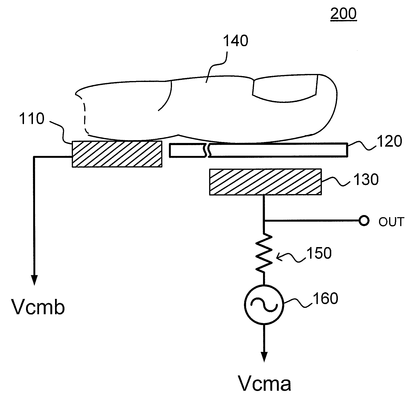
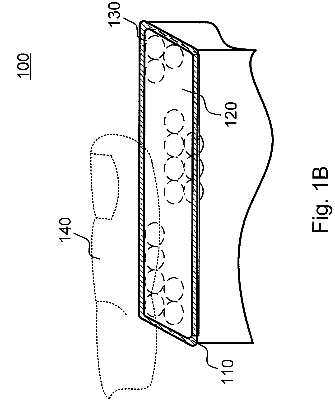
[0023]FIG. 2 shows a fingerprint sensing circuit according to the invention. The fingerprint sensing circuit 200 comprises the external electrode 110, the cover layer 120, a plurality of sensing units 130 (only one is shown for explanation), a resistor 150, and a signal source 160. The external electrode 110 and the signal source 160 are respectively coupled to the reference levels Vcmb and Vcma. Practically, Vcma and Vcmb may or may not be the same DC voltage level. The cover layer 120 covers the sensing unit 130. The sensing unit 130 is coupled to the signal source 160 through the resistor 150, and the fingerprint sensing circuit 100 further comprises an output node OUT coupled between the sensing unit 130 and the resistor 150. The signal source 160 is for providing a reference signal, such as an AC sinusoidal wave signal with a frequency range from 1 KHz to 1 MHz. The finger 140 contacts the external electrode 110 and the cover layer 120 and covers many sensing units 130. Actuall...

second embodiment

[0028]FIG. 8 shows the detailed circuit configuration of a fingerprint sensing circuit according to the claimed invention. The multiplexer (MUX) 810 of the fingerprint sensing circuit 800 is coupled to a plurality of capacitors 710 and is for selecting one of the capacitors 710. The selected capacitor 710 and the variable resistor 820 form a high-pass filter circuit to the signal source 660. FIG. 9 shows the relation between the frequency response of the high-pass filter and the reference signal in frequency domain. Similarly, the comparator 432 compares the detected result with a reference value Vref2 to generate an indication signal, and the indication signal controls the counter 434 to increase or decrease the value of the digital signal, which in turn controls the variable resistor 820 to change its resistance.

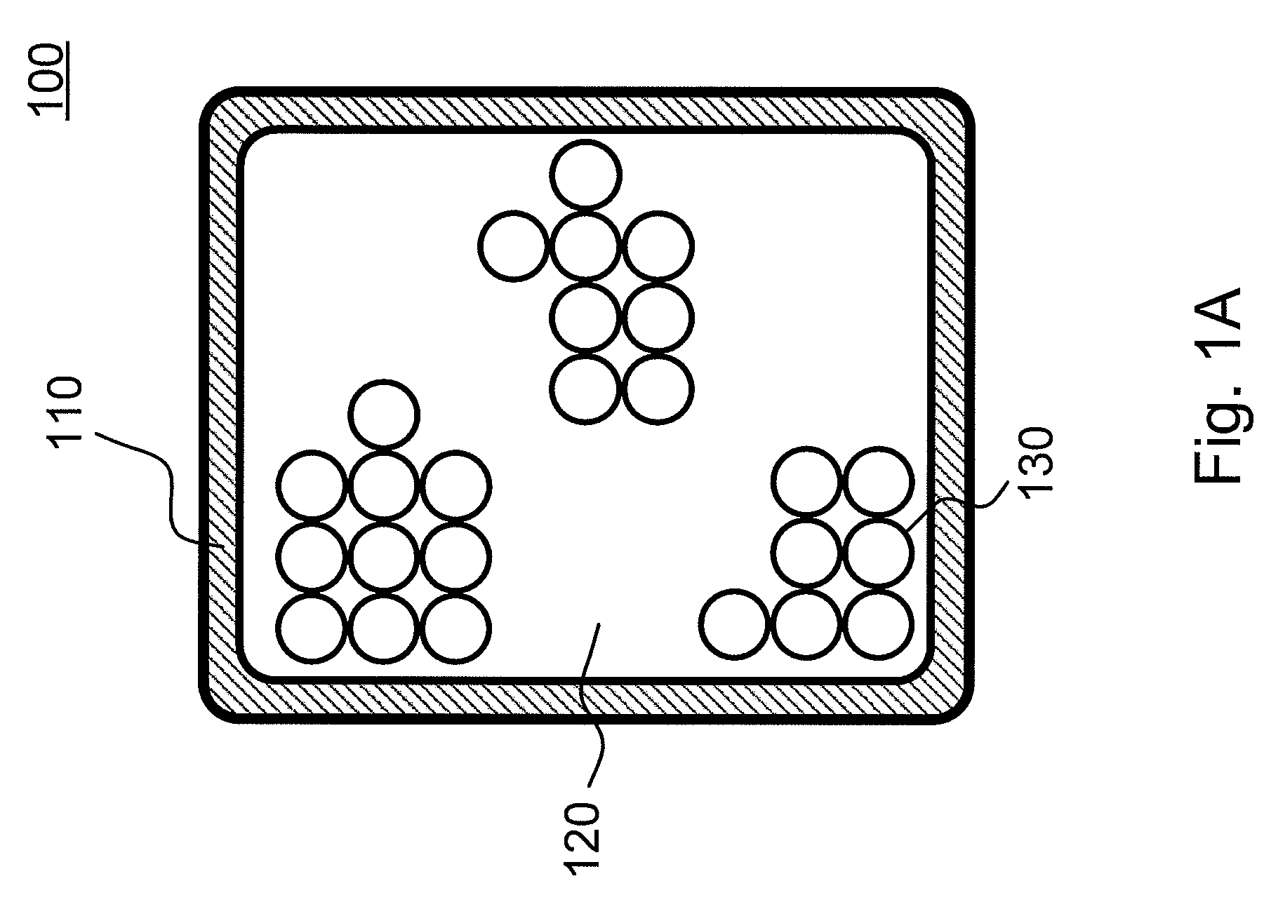
[0029]For the circuit layout, the structure of the sensing units can be embodied by the drawing shown in FIG. 10. For example, the shape of the sensing unit may be a circl...


PUM


Abstract

A fingerprint sensing circuit for detecting a fingerprint of a user, including a signal source, at least a sensing unit, a resistor, an electrode, and a detecting circuit. The signal source provides a reference signal. The electrode is coupled to a reference level. The sensing unit generates a sensed value according to the electrode and the fingerprint of the user. The resistor is coupled between the signal source and the output node. The detecting circuit is coupled to the output node. The resistor, the sensing unit, and the electrode constitute a filter circuit to the signal source. At least a first signal is generated to the output node according to the reference signal and the sensed value, and the detecting circuit detects the first signal to generate a corresponding detected result indicative of the fingerprint.

Description

FIELD OF THE INVENTION[0001]The present invention relates to a fingerprint sensing circuit.DESCRIPTION OF THE PRIOR ART[0002]At present, fingerprint recognition technology has become a common security mechanism, and therefore more and more fingerprint sensing circuits are proposed. For example, U.S. Pat. No. 4,210,899 and U.S. Pat. No. 4,525,859 provide methods for capturing fingerprints through optical scanning and video camera respectively. However, optical-based recognition methods may not work well if optical sensing devices are defaced and damaged, and may also be cheated by using pictures or patterns which have correct fingerprints thereon. In addition, U.S. Pat. No. 6,259,804 provides a method based on electric field for fingerprint sensing. In FIG. 12 of that patent, the sensed signal generated by the sensing electrode 78 is amplified by the amplifier 73, and the amplified signal is an AC analog signal which is then converted into a digital signal by an analog-to-digital con...

Claims


Application Information

Patent Timeline
IPC IPC(8): G06K9/00
CPCG06K9/0002G06V40/1306
Inventor PAI, HUNG-CHUANCHEN, SHOU-FANGYANG, CHAO-TUNG
Owner XUESHAN TECH INC
Why Eureka
Try Eureka