
Image processing circuit, display device, and printing device

a technology of image processing circuit and display device, which is applied in the direction of computing, instruments, and filling the planer surface with attributes, etc., and can solve problems such as the inability to achieve hatching processing

Inactive Publication Date: 2009-02-19
SEIKO EPSON CORP
View PDF4 Cites 15 Cited by
  • Summary
  • Abstract
  • Description
  • Claims
  • Application Information

AI Technical Summary

Benefits of technology

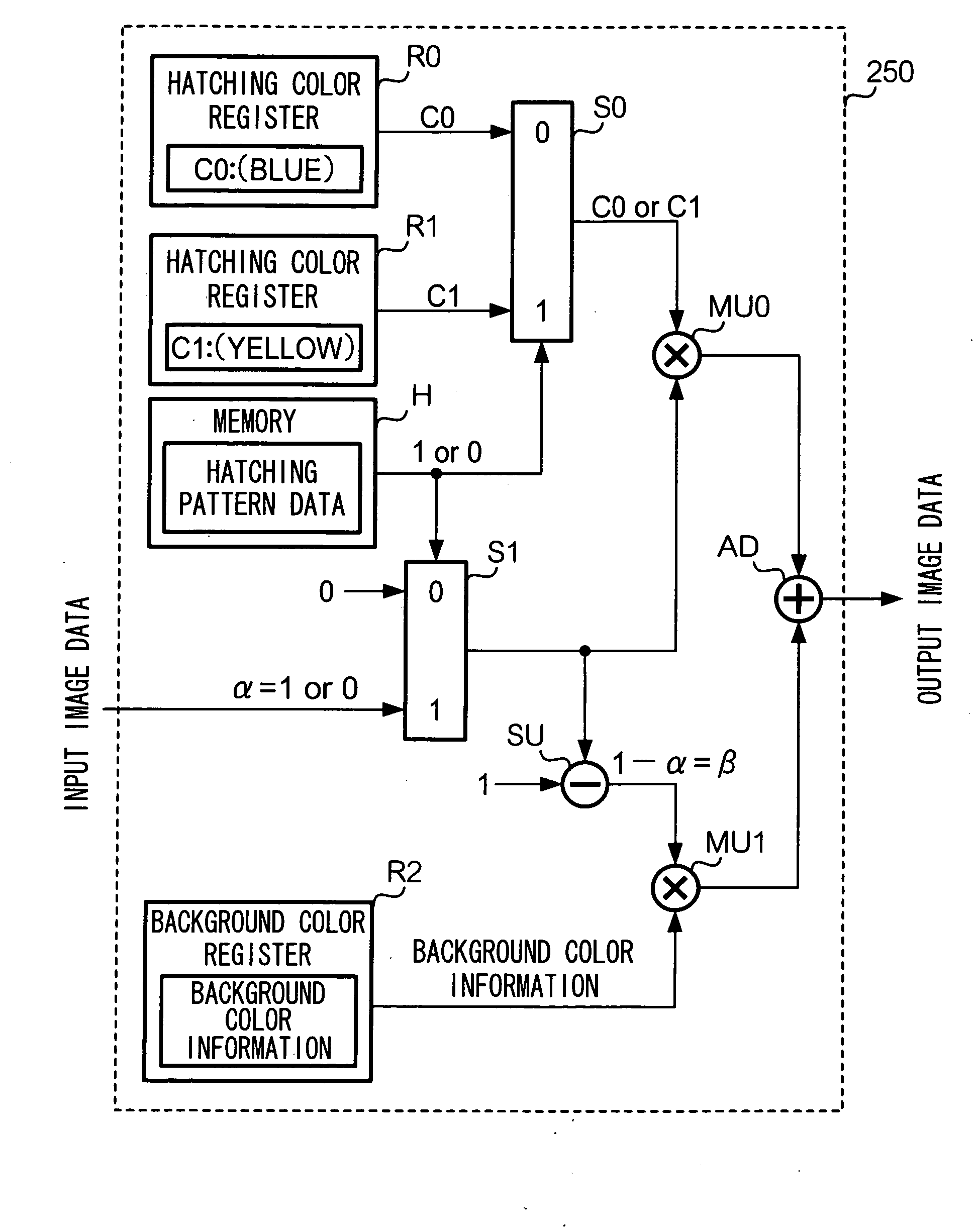
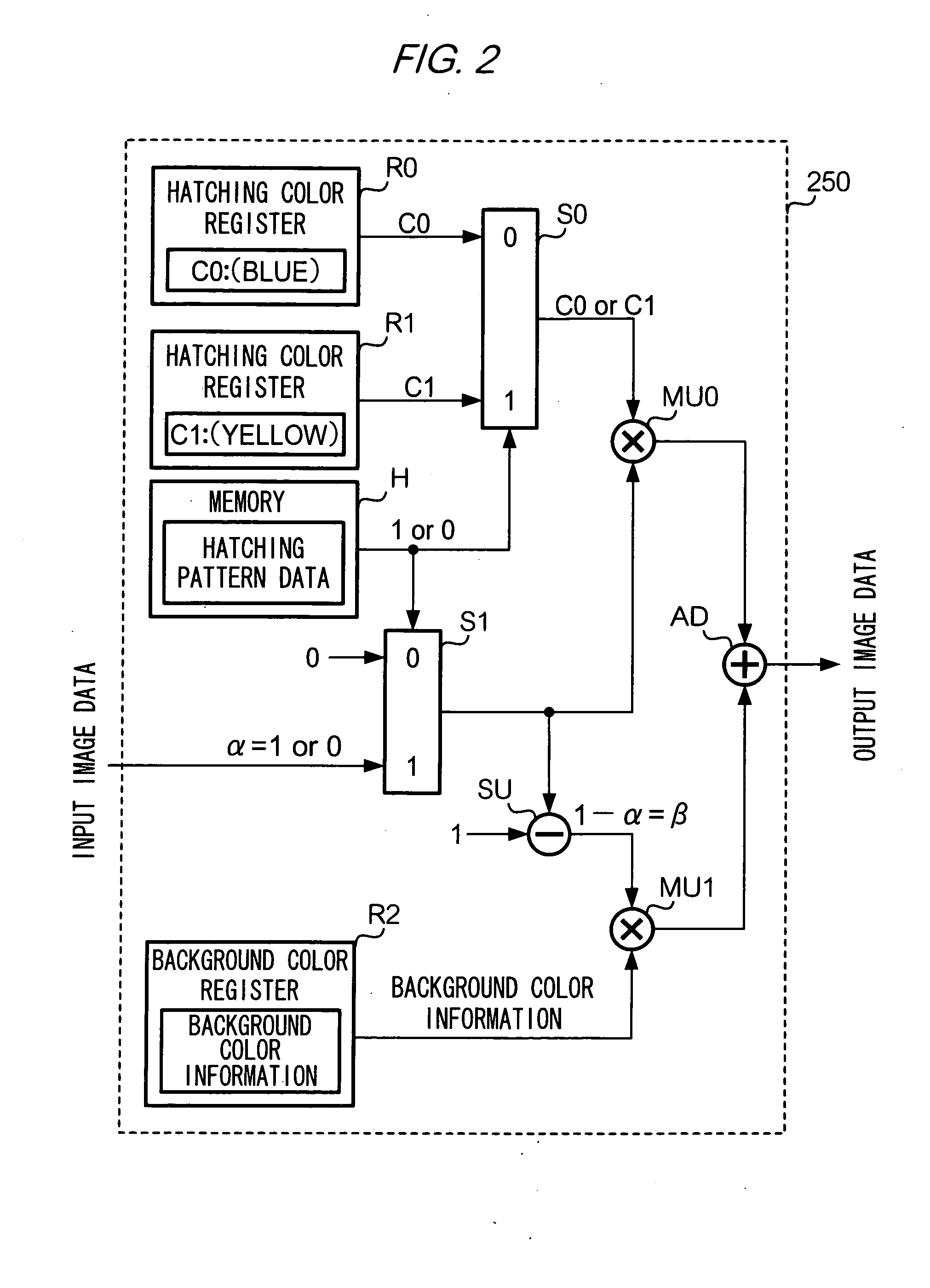
[0021]Accordingly, a hatching processing can be achieved so that plural shape-images are arrayed only in specified areas of an image expressed by binary image data, and that a background image is seen through parts of the specified areas. Further, an image obtained as a result of the hatching processing can be displayed.

Problems solved by technology

However, such a hatching processing cannot be achieved only by the technique disclosed in the aforementioned JP-A-5-210381 since this technique simply develops a predetermined block pattern in a specified area.

Method used


Image

  • Image processing circuit, display device, and printing device
  • Image processing circuit, display device, and printing device
  • Image processing circuit, display device, and printing device

Examples


Embodiment Construction

Exemplary Embodiment

[0036]In an exemplary embodiment described below, a processing for laying out plural shape-images arrayed in an image area will be referred to as “hatching”. The plural shape-images which are arrayed in this processing may all be the same as each other or different from each other. For example, a form of hatching known as “oblique line shading” can be achieved by laying out repeatedly at uniform intervals, line segment images extending in one identical direction. Another form of hatching commonly known as “cross shading” can be achieved by laying out repeatedly at uniform intervals, line segment images, respectively extending in two different directions. Yet another form of hatching can be achieved by laying out alternating shapes of a heart and a clover or by randomly laying out abstract shapes which are all different from each other. That is, shape-images used for hatching can be of any size or form, and any number of shape-images may be used for hatchings.

[003...


PUM


Abstract

An image processing circuit includes: a storage unit that stores positions of pixels constituting a shape-image to be regularly-arranged and pixel values of the pixels; a conversion unit that: if a pixel value of a first pixel constituting an image represented by input binary image data, the pixel value of the first pixel being expressible by one value or another value, one of the values being 0, and a pixel value of a second pixel constituting the shape-image and arranged at a position corresponding to a position of the first pixel is a predetermined value, converts the pixel value of the first pixel into 0 and outputs a pixel value 0; and if the pixel value of the first pixel is 0, or if the pixel value of the first pixel is a value other than 0, and the pixel value of the second pixel is a value other than the predetermined value, directly outputs the pixel value of the first pixel; a first multiplication unit that multiplies the pixel value of the second pixel by the pixel value output from the conversion unit, and outputs a resultant value; an inversion unit that inverts the pixel value output from the conversion unit and outputs a resultant value; a second multiplication unit that multiplies the pixel value of the first pixel or a pixel value of a third pixel constituting a background part of the image represented by the binary image data by the value output from the inversion unit, and outputs a resultant value; and an adder that adds up the value output from the first multiplication unit and the value output from the second multiplication unit, and outputs a resultant value as output image data.

Description

[0001]The entire disclosure of Japanese Patent Application No. 2007-211254 filed on Aug. 14, 2007 is expressly incorporated by reference herein.BACKGROUND[0002]1. Technical Field[0003]The present invention relates to a technique for laying out plural shapes in an array within an image area.[0004]2. Related Art[0005]In the field of image processing, there is a technique known as hatching processing. Hatching processing involves the laying out of plural shapes in an array within an image area which is defined as a text area, a table, or a figure. In other words, the technique of hatching processing is a process of patterning or a form of shading. For example, JP-A-5-210381 discloses a technique for rapidly developing a hatching pattern on a frame memory by using a BiTBLT (bit boundary / block transfer) circuit which repeatedly transfers a block pattern for hatching within a specified area.[0006]In the hatching processing as described above, it is necessary to employ wide variations of h...

Claims


Application Information

Patent Timeline
IPC IPC(8): G06K9/00
CPCG06F3/13G06F3/14G06T11/40G09G5/024G09G5/393G09G5/30G09G5/363G09G5/37G09G5/24
Inventor ONO, YOSHIYUKISAWAZAKI, TAKASHISAITO, AKIRA
Owner SEIKO EPSON CORP
Learn More