

Semiconductor device and manufacturing method thereof
a semiconductor and manufacturing method technology, applied in the direction of semiconductor devices, semiconductor/solid-state device details, electrical apparatus, etc., can solve the problems of damage to the extended portion of the semiconductor elements positioned on the upper side, and the normal wire bonding is not performed
- Summary
- Abstract
- Description
- Claims
- Application Information
AI Technical Summary
Benefits of technology
Problems solved by technology
Method used
Image

Examples
first embodiment
[0090]A first embodiment of the semiconductor device accord will be described with reference to FIGS. 1A through 9B.
[0091]The semiconductor device according to the present embodiment comprises a first semiconductor element which is mounted on a wiring board serving as a supporting base in a face-up state, with an external connection electrode terminal of the first semiconductor element being connected to an electrode terminal on the wiring board with a wire bonding method; and a second semiconductor element which is mounted on the first semiconductor element in a face-up state, with an external connection electrode terminal of the second semiconductor element being connected to an electrode terminal on the wiring board with a wire bonding method.
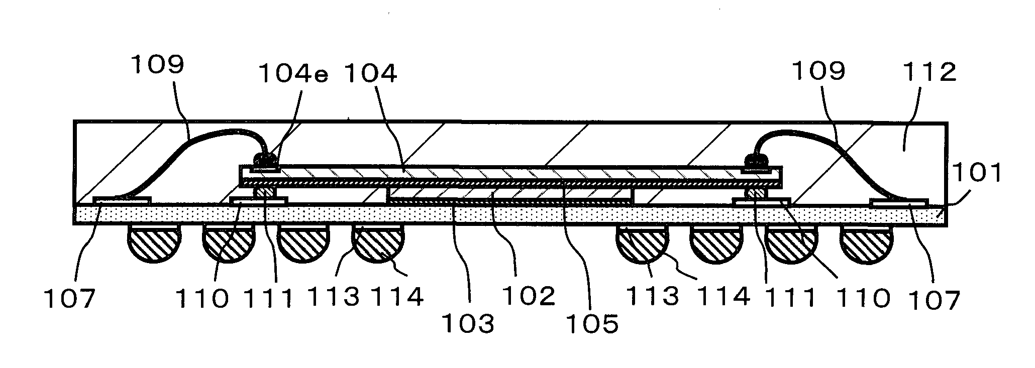
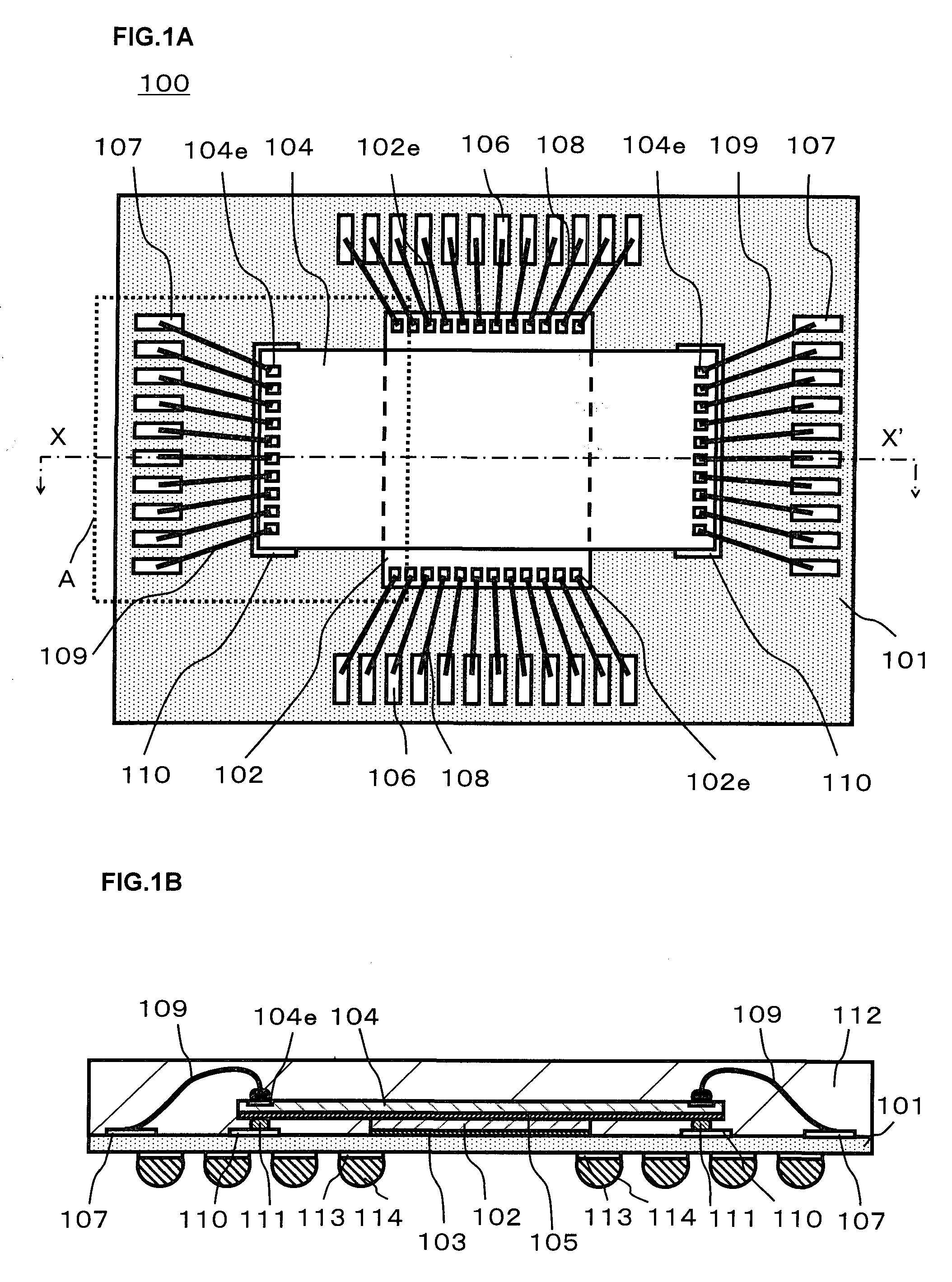
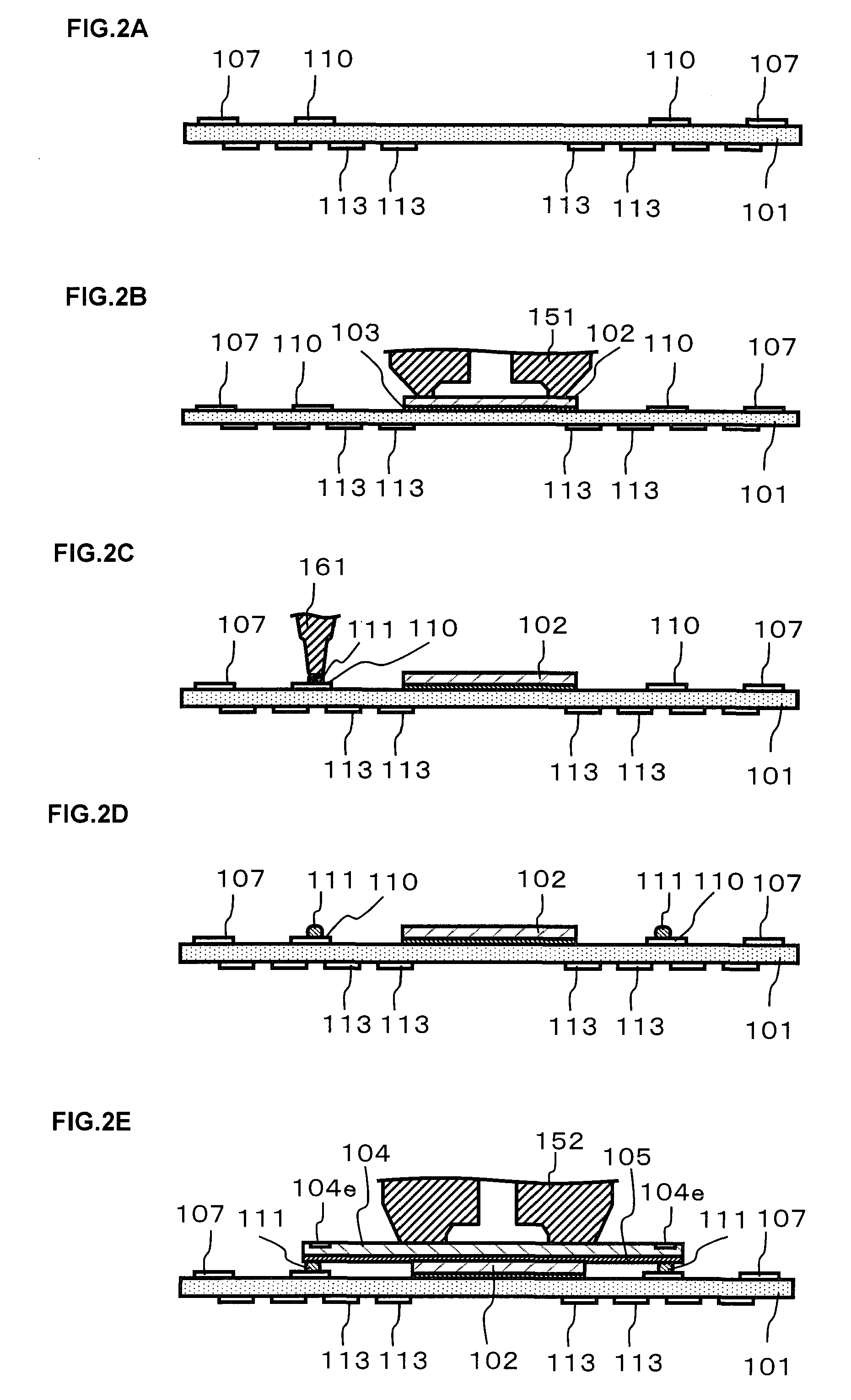
[0092]A semiconductor device 100 according to the first embodiment is shown in FIGS. 1A and 1B.
[0093]FIG. 1A shows a plan view of the semiconductor device 100, and FIG. 1B shows an X-X′ cross-section of FIG. 1A. Note that in FIG. 1A, display...
second embodiment
[0231]A second embodiment of the semiconductor device according will be described with reference to FIGS. 9A through 13B.
[0232]The semiconductor element according to the present embodiment is mounted in a face-down (flip-chip) state on a wiring board which is a supporting base, and comprises a first semiconductor element wherein external connection bump electrodes thereof are connected to electrode terminals on the wiring board, and a second semiconductor element which is mounted on the first semiconductor element in a face-up state, wherein an electrode terminal pad thereof is connected to the electrode terminals on the wiring board with a wire bonding method.
[0233]A semiconductor device 200 according to the second embodiment is shown inFIGS. 9A and 9B.
[0234]FIG. 9A shows a flat surface of the semiconductor device 200, and FIG. 9B shows an X-X′ cross-section of FIG. 9A. Note that in FIG. 9A, display of a resin sealing portion is omitted, and the external form thereof is shown with ...
third embodiment
[0288]A third embodiment of the semiconductor element will be described with reference to FIGS. 14A through 22B.
[0289]The semiconductor device according to the third embodiment comprises a first semiconductor element which is mounted on a wiring board serving as a supporting base in a face-up state, with an external connection electrode terminal of the first semiconductor element being connected to an electrode terminal on the wiring board with a wire bonding method; a second semiconductor element which is mounted on the first semiconductor element in a face-up state, with an external connection electrode terminal of the second semiconductor element being connected to an electrode terminal on the wiring board with a wire bonding method; and a third semiconductor element which is mounted on the second semiconductor element in a face-up state, with an external connection electrode terminal of the third semiconductor element being connected to an electrode terminal on the wiring board ...
PUM
 Abstract
Description
Claims
Application Information