Check patentability & draft patents in minutes with Patsnap Eureka AI!

Image sensor and method of manufacturing the same

Active Publication Date: 2009-04-02
DONGBU HITEK CO LTD
View PDF3 Cites 2 Cited by
  • Summary
  • Abstract
  • Description
  • Claims
  • Application Information

AI Technical Summary

Benefits of technology

[0013]Because the isolation region in the disclosed embodiments is formed under the peripheral region, an improved electric isolation effect between the pixel array and the peripheral region may be attained so that leakage and noise between the two regions are reduced or removed, thereby improving performance, yield, and reliability of an image sensor product.
[0014]In addition, since the substrate resistances of NMOS and PMOS transistors in the peripheral region are reduced in the disclosed embodiments, speed and body effect may be reduced in terms of device performance.

Problems solved by technology

In the conventional art, however, it is difficult to completely isolate an epitaxial layer in the pixel array from that in the peripheral region.

Method used


Image

  • Image sensor and method of manufacturing the same
  • Image sensor and method of manufacturing the same
  • Image sensor and method of manufacturing the same

Examples


Embodiment Construction

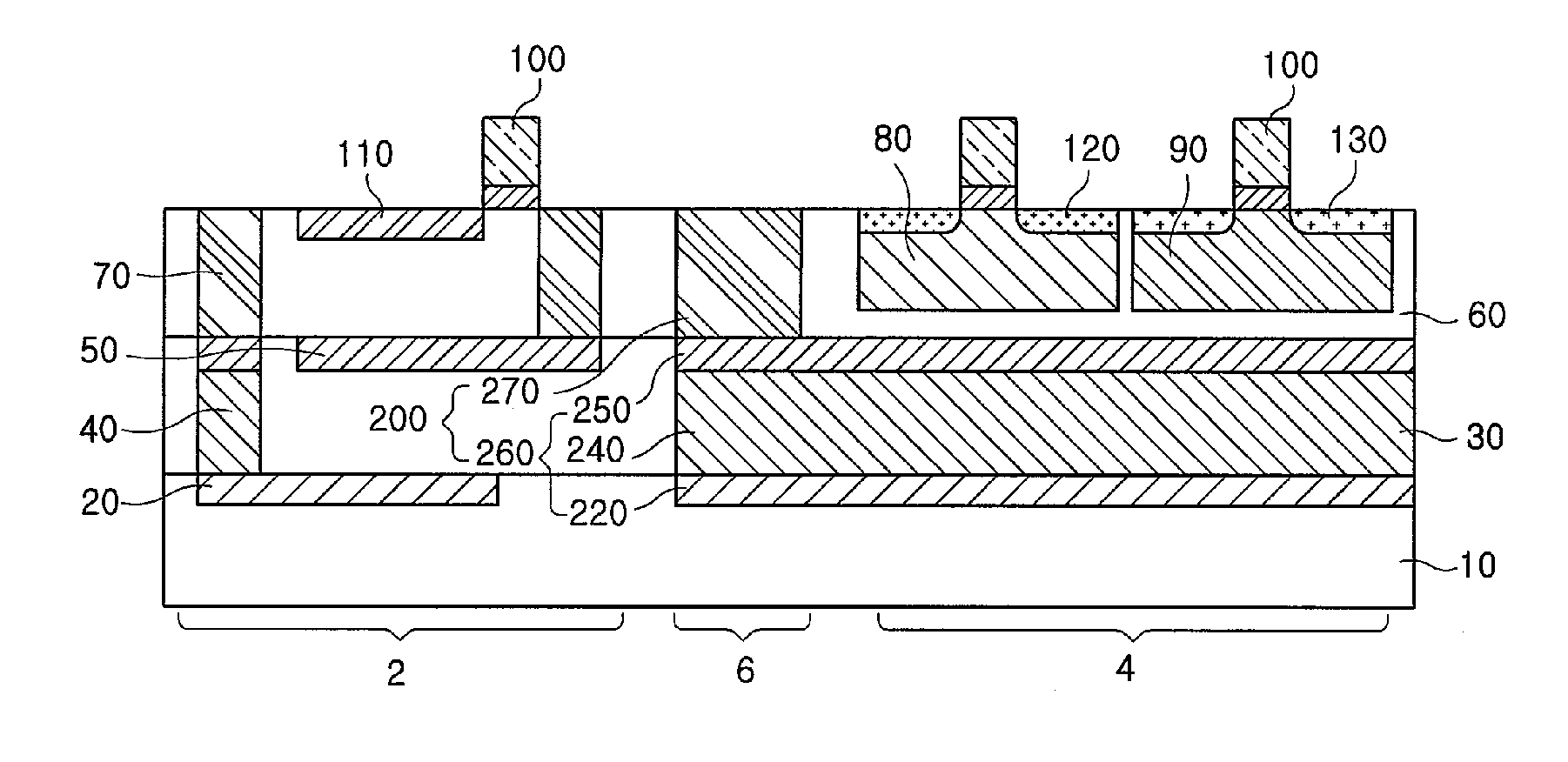
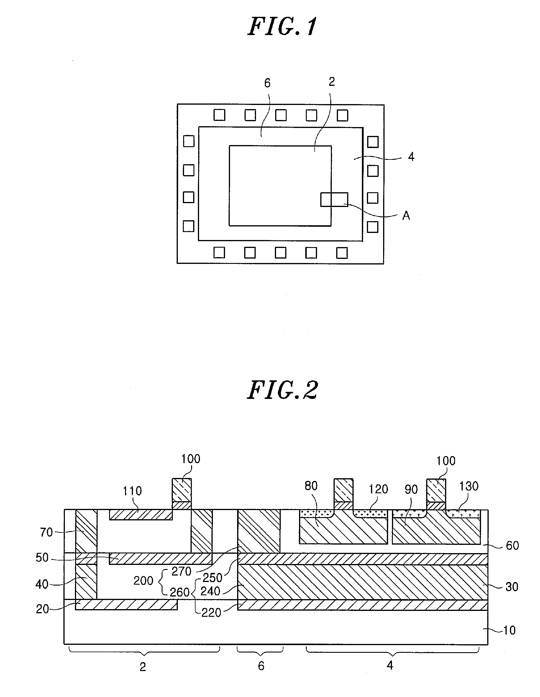
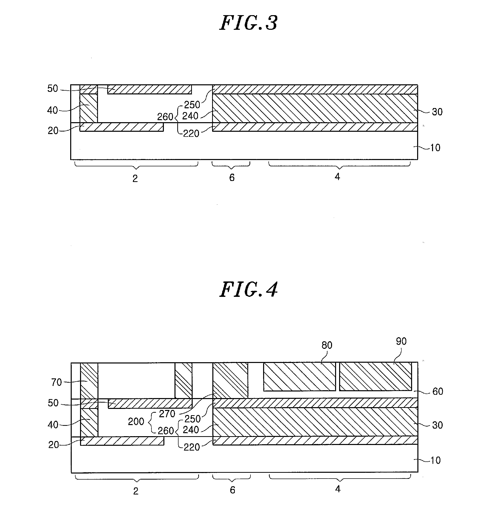
[0010]In general, example embodiments of the invention relate to an image sensor capable of electrically isolating a pixel array including a photodiode from a peripheral region including a circuit for processing signals in a vertical-type CMOS image sensor and a method of manufacturing the same.

[0011]In accordance with a first embodiment, there is provided an image sensor, comprising a pixel array including a photodiode; a peripheral region including a logic circuit; and an isolation region formed between the pixel array and the peripheral region and formed under the peripheral region to electrically isolate the pixel array from the peripheral region.

[0012]In accordance with another embodiment, there is provided a method of manufacturing an image sensor comprised of a pixel array region, an isolation region and a peripheral region, the method comprising forming a pixel array within the pixel array region; forming a first isolation region to be electrically isolated from the pixel ar...


PUM


Abstract

An image sensor includes a pixel array including a photodiode, a peripheral region including a logic circuit, and an isolation region formed between the pixel array and the peripheral region and formed under the peripheral region to electrically isolate the pixel array from the peripheral region.

Description

CROSS-REFERENCE TO RELATED APPLICATION[0001]This application claims priority to Korean Application No. 10-2007-0097282, filed on Sep. 27, 2007, which is incorporated herein by reference in its entirety.BACKGROUND[0002]1. Field of the Invention[0003]Embodiments of the present invention relate to an image sensor and a method of manufacturing the same.[0004]2. Description of Related Art[0005]In general, an image sensor formed as a semiconductor device for converting an optical image into an electric signal may include a charge coupled device (CCD) or a complementary metal oxide silicon (CMOS) image sensor (CIS).[0006]A CIS may include a pixel array, each unit pixel in the array including a photodiode and a MOS transistor formed therein. Electric signals of each unit pixel may sequentially be detected by a switching method to detect an image.[0007]The conventional CIS device may include a pixel array including photodiodes and a peripheral region including a logic circuit.[0008]In the im...

Claims


Application Information

Patent Timeline
IPC IPC(8): H01L27/146H01L31/18
CPCH01L27/14645H01L27/1463H01L27/146H01L27/14
Inventor LIM, SU
Owner DONGBU HITEK CO LTD
Features
  • R&D
  • Intellectual Property
  • Life Sciences
  • Materials
  • Tech Scout
  • Unparalleled Data Quality
  • Higher Quality Content
  • 60% Fewer Hallucinations
Learn More