Traveling-Wave Tube 2D Slow Wave Circuit

a technology of slow wave and travel wave tube, which is applied in the direction of travel wave tube, electric discharge tube, electrical apparatus, etc., can solve the problems of unable to build beam tunnels across waveguides, non-overlapping or intermeshed parts in functional circuits, etc., and achieves simple fabrication, wide instantaneous bandwidth capability, and high power

Inactive Publication Date: 2009-04-16
BARNETT LARRY R +1
View PDF10 Cites 29 Cited by
  • Summary
  • Abstract
  • Description
  • Claims
  • Application Information

AI Technical Summary

Benefits of technology

[0017]The present invention establishes a circuit configuration wherein the vanes do not overlap to produce a microwave signal that is essentially confined to the electron beam tunnel where it is highly interactive. This circuit is useful for making improved millimeter and sub-millimeter wave amplifiers or oscillators in that it has higher power and wider instantaneous bandwidth capability than previous circuits, dimensional tolerance, simple fabrication, mode stability, very low loss, high efficiency, and excellent thermal and mechanical ruggedness.
[0018]The circuit vanes do not overlap in the present invention and this feature allows for the electron beam to be relatively much larger. The present invention permits higher-current, sheet-electron beams to be used that can be essentially, the full width of the circuit, with much higher current and power, and the tube power to be much larger than for any prior art microwave traveling wave tube at similar frequency.
[0019]The prior art difficulties in cutting a hole for the electron beam tunnel, or a making a spiral for the radio frequency (RF) signal, is now eliminated. The present invention makes it easy to manufacture a circuit for very short wavelengths (very high frequency).
[0020]Another advantage of the present invention is that the output power level and bandwidth can be systematically adjusted by a dimensional change in the circuit.
[0021]Another advantage of the present invention is that the overmoding issue is avoided (i.e. the generation of undesirable modes which results in spurious signals), which usually arises in conventional high-aspect-ratio structures. The present invention makes it relatively easy to design a high aspect ratio sheet electron beam amplifier or oscillator.
[0022]The present invention enables the use of a sheet electron beam in a microwave tube and this has advantages in considerably reducing beam density required in the interaction, and, simultaneously reducing the RF power density on the circuit, magnetic focusing requirements, and cathode current density loading.

Problems solved by technology

Having non-overlapping or intermeshed parts in a functional circuit was thought to be impossible.
However, despite many attempts and progress to three-dimensionally micro-fabricate folded waveguide traveling-wave-tube circuits, construction of the beam tunnel across the waveguides has always been problematic.

Method used


Image

  • Traveling-Wave Tube 2D Slow Wave Circuit
  • Traveling-Wave Tube 2D Slow Wave Circuit
  • Traveling-Wave Tube 2D Slow Wave Circuit

Examples


example

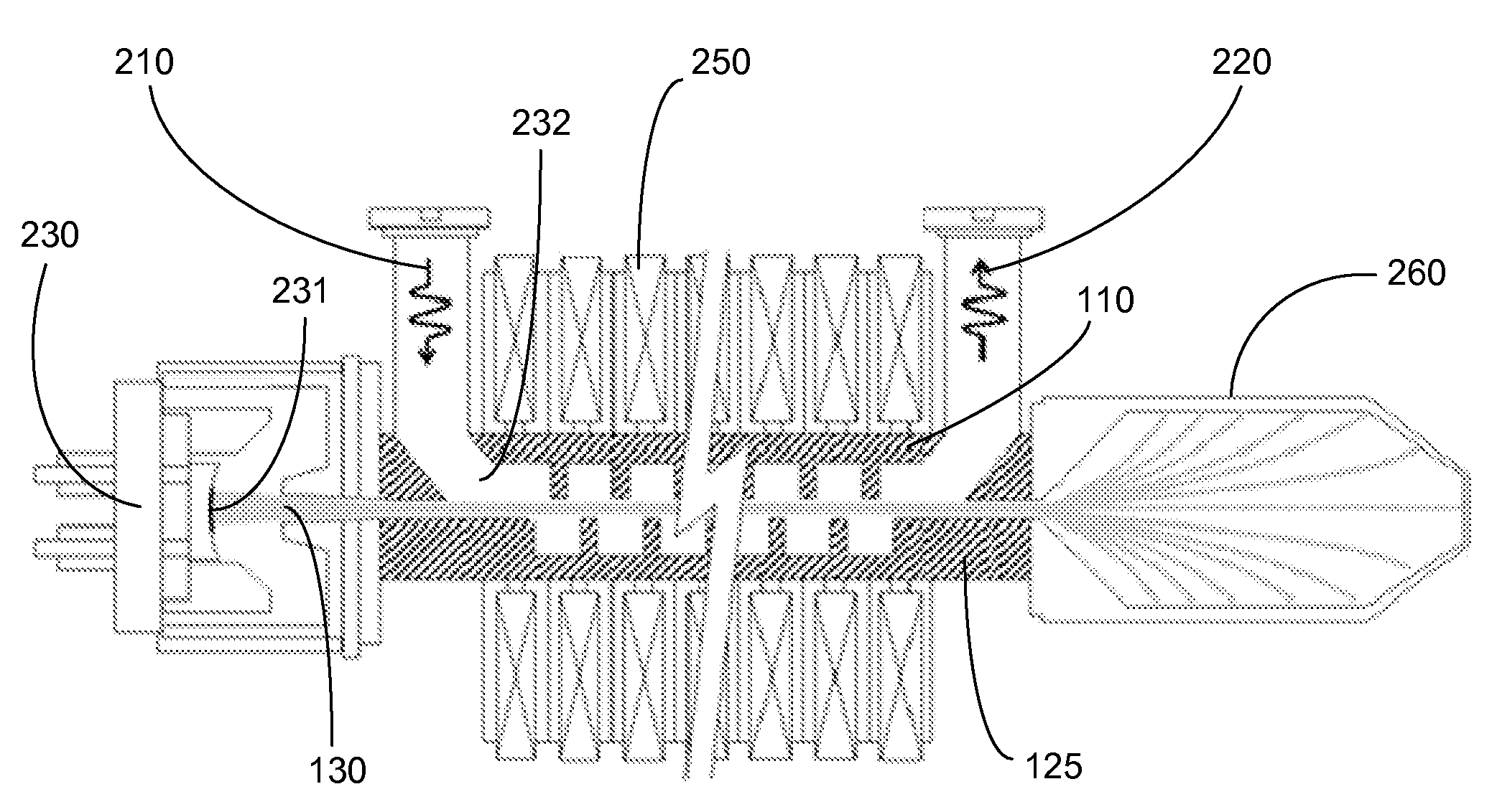
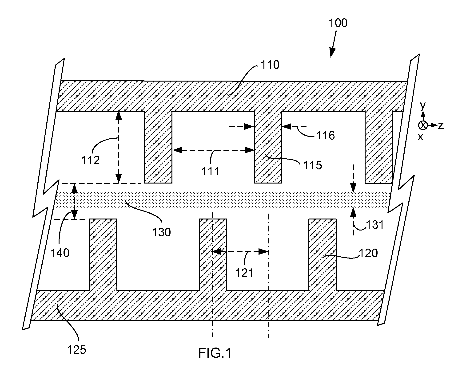
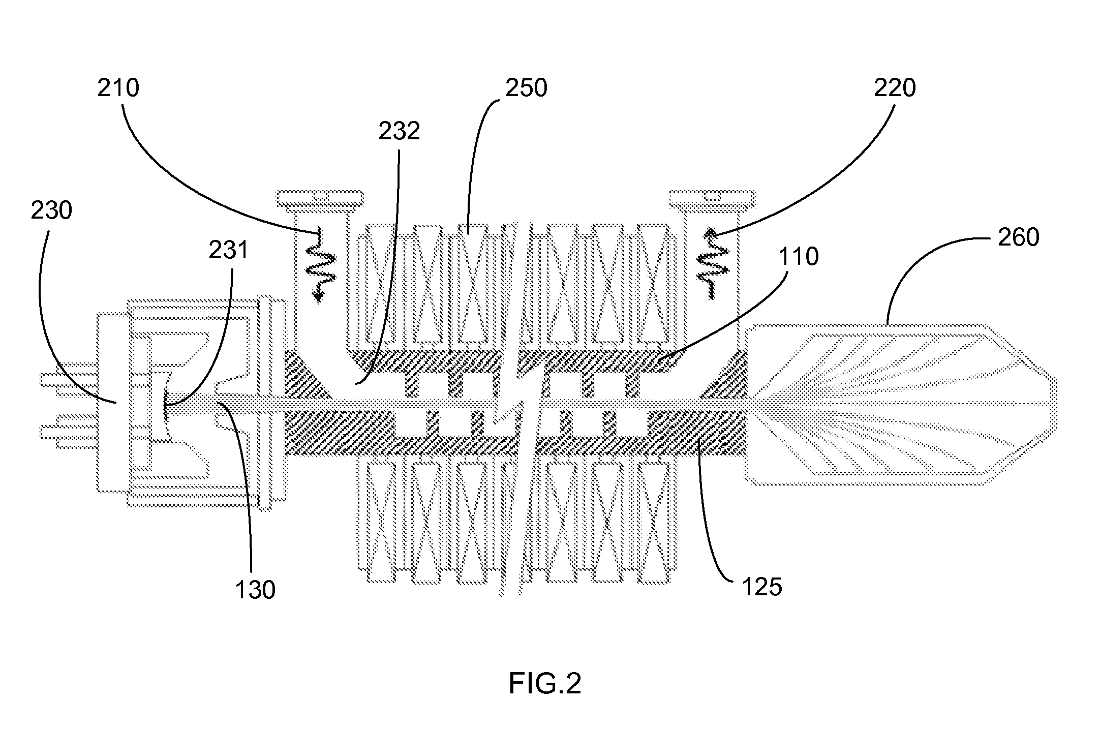
[0051]The circuit of the invention has been tested in a traveling wave tube comprising a center frequency of 220 GHz, wherein the sheet electron beam has a width to height of 7 to 1, is 0.100 millimeters thick and 0.700 millimeters wide wherein the electrically conductive material of the solid-body is copper, the length is 38 millimeters; all of the vanes are configured with a period of 0.46 millimeters, a thickness of 0.115 millimeters, a height of 0.270 millimeters and a width of 0.770 millimeters; and, the tunnel is 0.150 millimeters in height. Thus, the sheet electron beam fills 67% of the tunnel (the sheet beam size is 0.700 millimeters (x) by 0.100 millimeters (y), which corresponds to a 7:1 aspect ratio).

[0052]The example dimensions are tentatively designed for the first space harmonic (n=1) operation with a 20 kilovolt electron beam, though operation in the fundamental (n=0) space harmonic can be accomplished with shorter period. The advantage of the n=1 operation is that th...


PUM


Abstract

A two-dimensional circuit for a traveling-wave tube for millimeter and sub-millimeter electromagnetic waves synchronously interacts with an electron beam in a vacuum electronic microwave amplifier or oscillator. The circuit is a solid body having a length along the tube axis. The solid body has an electrically conductive top section and an electrically conductive bottom section. The top section is configured with a plurality of vertical vanes having a width and height and configured parallel to each other. The bottom section is similarly configured such that when the circuit is viewed in cross section along the length, the vanes on the bottom section are staggered with respect to the vanes on the top section. The top section and the bottom section are separated from each other to define a tunnel through the solid body along the length.

Description

CROSS-REFERENCE TO RELATED APPLICATIONS[0001]This application claims the benefit of the filing date of prior-filed U.S. provisional application 60 / 979,392, filed 12 Oct. 2007, which is hereby incorporated by reference herein.TECHNICAL FIELD[0002]In the field of amplifiers and oscillators, a traveling wave tube interaction circuit having means therein for propagating an electromagnetic wave or component thereof at a velocity reduced from the free space velocity of the wave and propagated in proximity to an electron stream, permitting exchange of energy between the electrons and the electromagnetic wave.BACKGROUND ART[0003]Conventional traveling-wave tubes utilize a slow wave structure through which an electron beam passes. In the traveling-wave tube, electrons in the beam travel with velocities slightly greater than that of a radio frequency wave, and on the average are slowed down by the field of the wave. A loss of kinetic energy of the electrons appears as increased energy conveye...

Claims


Application Information

Patent Timeline
Patent Type & Authority Applications(United States)
IPC IPC(8): H01J25/34
CPCH01J25/34H01J23/20
Inventor BARNETT, LARRY R.SHIN, YOUNG-MIN
Owner BARNETT LARRY R
Why Eureka
Try Eureka