El display device

a technology of display device and display circuit, which is applied in the direction of lighting apparatus, instruments, light sources, etc., can solve the problems of large adjustment time, large amount of adjustment time, and large power supply circuit such as a power supply i

Inactive Publication Date: 2009-04-30
TOSHIBA MATSUSHITA DISPLAY TECH
View PDF5 Cites 132 Cited by
  • Summary
  • Abstract
  • Description
  • Claims
  • Application Information

AI Technical Summary

Benefits of technology

[0012]According to the embodiment of the invention, it is possible to measure or monitor a current flowing through a power supply wiring without physically changing or operating a mechanism or the like of the power supply wiring.

Problems solved by technology

Due to the introduction of these mechanisms, there has been a problem in that a cost of the EL display device is increased, and a large amount of adjustment time is required.
However, in the event that the power supply circuit is designed in such a way as to be able to pass the maximum current used, there has been a problem in that a power supply circuit such as a power supply IC becomes very large.
Also, there has been a problem in that a long time is required for a defect inspection or characteristic evaluation of the EL display panel.

Method used


Image

  • El display device
  • El display device
  • El display device

Examples


embodiment

Details of Embodiment

[0103]Hereafter, a description will be given of details of the EL display device of the embodiment.

1. Configuration of Gate Drive Circuits

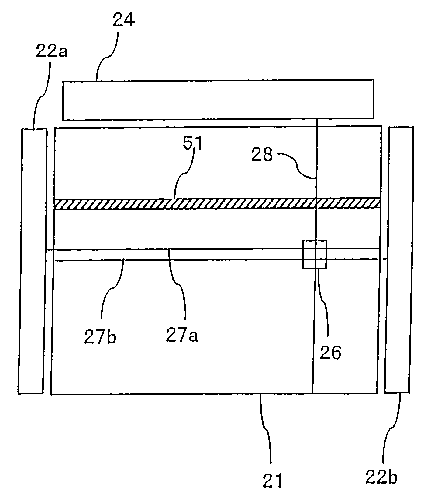
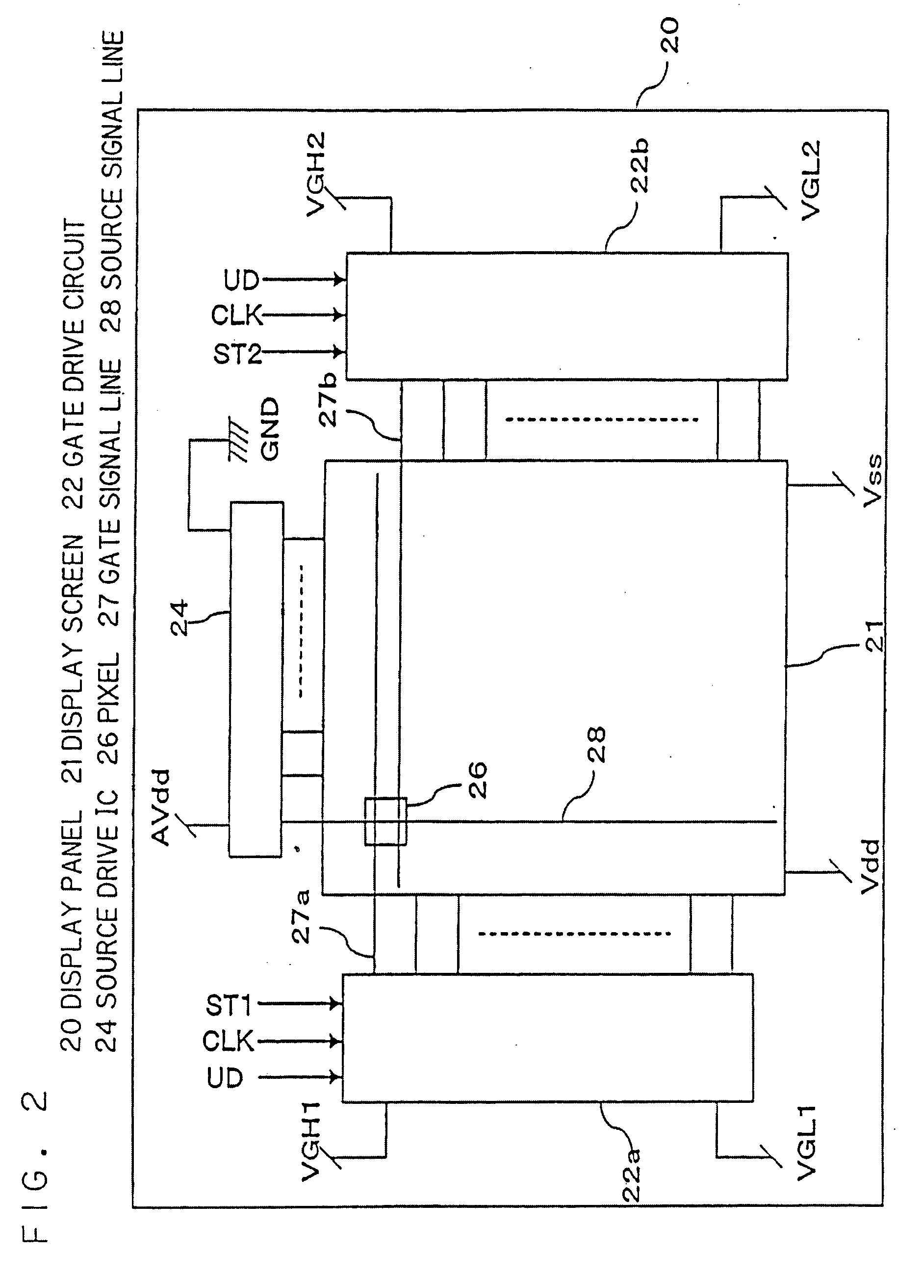
[0104]A description will be given of gate drive circuits 22 of the EL display device.

[0105]As shown in FIG. 2, a gate drive circuit 22a is provided at a left end of a display screen 21, while a gate drive circuit 22b is provided at a right end. It is sufficient that the gate drive circuits 22 are formed in a vacant area of a display panel.

1-1. Outline

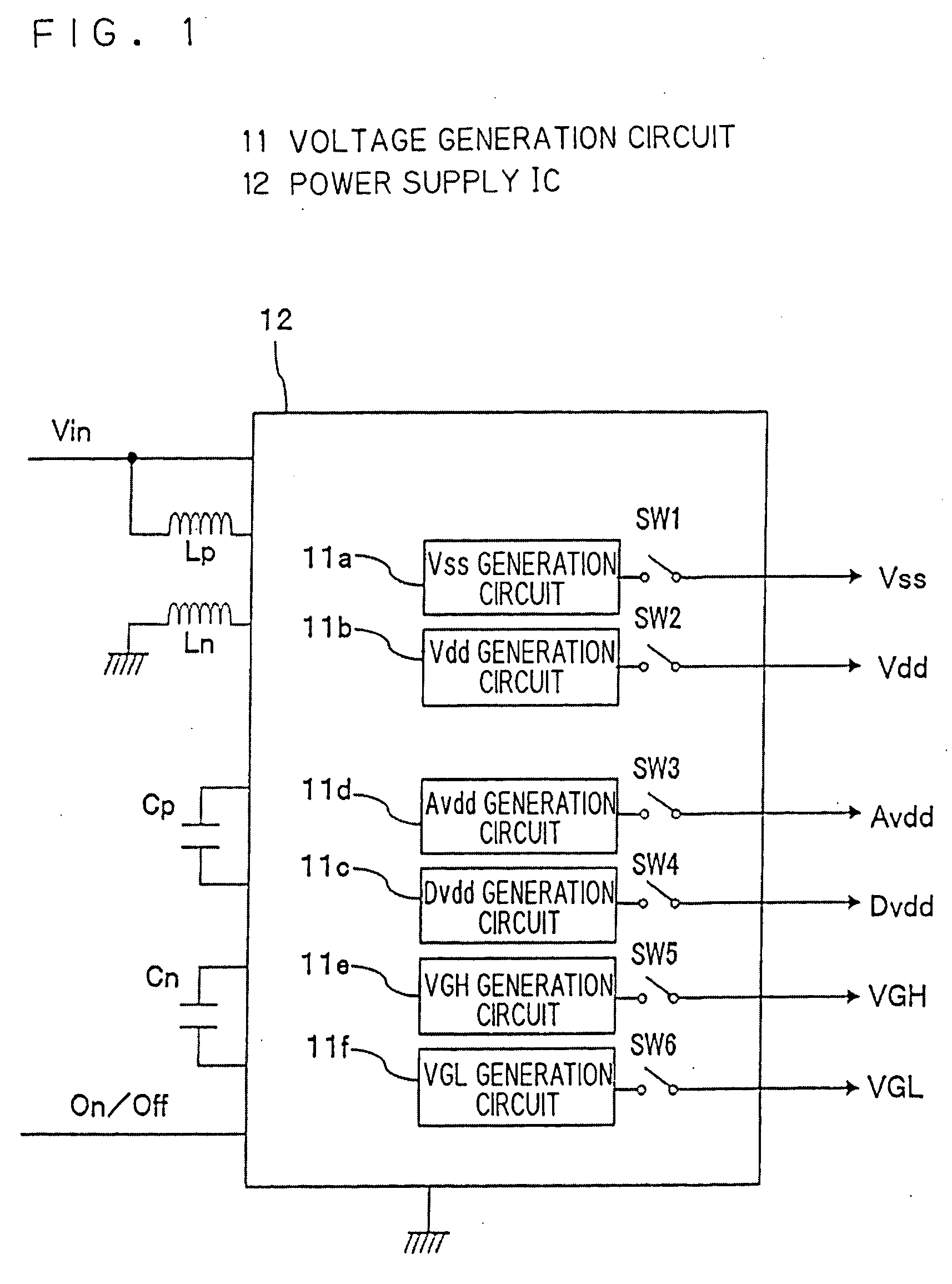
[0106]The gate drive circuit 22a controls a gate signal line 27a, while the gate drive circuit 22b controls a gate signal line 27b. On voltages (VGL) of the gate signal lines 27 and off voltages (VGH) of the gate signal lines 27 are supplied to the gate drive circuits 22a and 22b. The off voltages (VGH) are voltages which are equal to or higher than, or approximate to, an anode voltage Vdd. The on voltages (VGL) are voltages which are approximate to a cathode voltage Vss or a grou...

modification example 1

25-1. Modification Example 1

[0519]FIG. 72A shows a modification example of FIG. 3. In the configuration of FIG. 72A, one terminal of a capacitor 39 is connected to a Vsd voltage. That is, the anode voltage Vdd connected to one terminal of the drive transistor 31a is made different from the voltage Vsd connected to the capacitor 39.

[0520]With the kind of configuration of FIG. 72A, by the voltage Vsd applied to the capacitor 39 being separated from the anode voltage Vdd, no influence of a fluctuation in the anode voltage Vdd due to a change of the image display is suffered. Consequently, a voltage maintenance of the gate terminal of the drive transistor 31a becomes effective. The Vsd voltage is changed at a time of the defect inspection (or other inspections) of the EL display device. On changing the Vsd voltage, the cathode current or the anode current is changed, and it is possible to effectively inspect a pixel characteristic or defect by means of a magnitude of the current, a rate...

modification example 2

25-2. Modification Example 2

[0521]The heretofore described configuration of FIG. 72A can also be applied to the pixel of FIG. 72B.

[0522]In FIG. 72B too, the Vsd voltage, which differs from the anode voltage Vdd, is applied to one terminal of the capacitor 39. Consequently, no influence of a voltage change of the anode voltage Vdd is suffered.


PUM


Abstract

A switch being turned off using an output open function of a power supply circuit, a cathode voltage Vss is not transmitted, an output terminal takes on a high impedance condition and, a probing being done into a pad of the cathode voltage Vss output terminal with a probe, an ammeter which measures a current is disposed between the probe 304 and an external power source Vsst, making an adjustment time cathode voltage Vsst equal to an image display time cathode voltage Vss.

Description

TECHNICAL FIELD[0001]The present invention relates to an EL display device using a light-emitting display device such as an EL display panel (display device) using an organic or inorganic electroluminescence (EL) element or the like.BACKGROUND OF THE INVENTION[0002]An active matrix type image display device using an organic EL material or an inorganic EL material as an electrooptical transformation substance is of a light-emitting type whose emission luminance changes in response to a current written to a pixel, and which also has a light-emitting element in each pixel. The EL display device has advantages when compared with a liquid crystal panel, such as a high image visibility, a high luminous efficiency, no need for a backlight, and a high response speed.[0003]To date, regarding an organic EL (PLED, OLED or OEL) panel, an active matrix system has been actively developed. This system, being one which controls a current flowing through a light-emitting element inside each pixel ci...

Claims


Application Information

Patent Timeline
Patent Type & Authority Applications(United States)
IPC IPC(8): G09G3/30
CPCG09G3/006G09G3/3233G09G2320/0693G09G2300/0861G09G2300/0819G09G3/20G09G3/30G09G3/32H05B33/12
Inventor TAKAHARA, HIROSHI
Owner TOSHIBA MATSUSHITA DISPLAY TECH
Why Eureka
Try Eureka