Phase-Changeable Memory Devices Having Reduced Susceptibility to Thermal Interference

a phase-changeable memory and thermal interference technology, applied in the field of integrated circuit memory devices, can solve the problems of semiconductor device reliability, greater interference between adjacent cells, and different phase-changeable memory devices from dram and fram in terms of information programming methods

Active Publication Date: 2009-05-21
SAMSUNG ELECTRONICS CO LTD
View PDF3 Cites 65 Cited by
  • Summary
  • Abstract
  • Description
  • Claims
  • Application Information

AI Technical Summary

Problems solved by technology

However, the phase-changeable memory device is different from DRAM and FRAM in terms of an information programming method.
Since a semiconductor device has been being highly in

Method used


Image

  • Phase-Changeable Memory Devices Having Reduced Susceptibility to Thermal Interference
  • Phase-Changeable Memory Devices Having Reduced Susceptibility to Thermal Interference
  • Phase-Changeable Memory Devices Having Reduced Susceptibility to Thermal Interference

Examples


Embodiment Construction

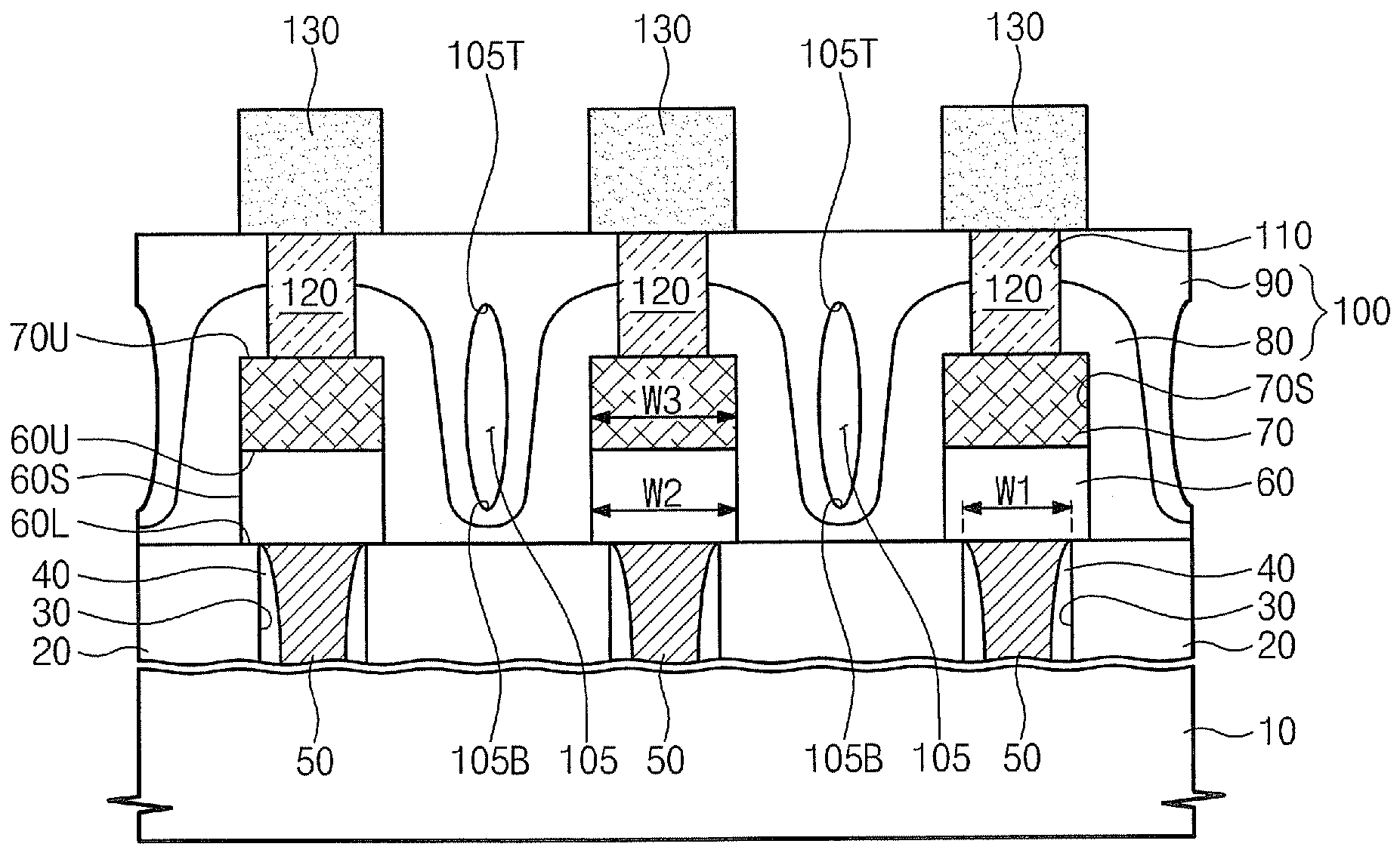
[0020]Hereinafter, embodiments of the present invention will be described in more detail with reference to the accompanying drawings. The objective(s), feature(s), and advantage(s) of the present invention will be thoroughly and easily understood with reference to the embodiments below and the accompanying drawings. The embodiments of the present invention may, however, be embodied in different forms and should not be construed as being limited to the embodiments set forth herein. Rather, these embodiments are provided so that this disclosure will be thorough and complete, and will fully convey the scope of the present invention to those skilled in the art. Like reference numerals refer to like elements throughout.

[0021]In the specification, ‘a substrate’ or ‘a semiconductor substrate’, or ‘a semiconductor layer’ may indicate an arbitrary semiconductor based structure having a silicon surface. Also, it may indicate an arbitrary conductive region and / or a semiconductor based structur...


PUM


Abstract

A non-volatile memory array includes an array of phase-changeable memory elements that are electrically insulated from each other by at least a first electrically insulating region extending between the array of phase-changeable memory elements. The first electrically insulating region includes a plurality of voids therein. Each of these voids extends between a corresponding pair of phase-changeable memory cells in the non-volatile memory array and, collectively, the voids form an array of voids in the first electrically insulating region.

Description

REFERENCE TO PRIORITY APPLICATION[0001]This U.S. non-provisional patent application claims priority under 35 U.S.C. §119 to Korean Patent Application No. 10-2007-0116666, filed Nov. 15, 2007, the entire contents of which are hereby incorporated herein by reference.FIELD OF THE INVENTION[0002]The present invention relates to integrated circuit memory devices and, more particularly, to non-volatile integrated circuit memory devices.BACKGROUND OF THE INVENTION[0003]The exemplary embodiments disclosed herein relates to a memory device, and more particularly, to a phase-changeable memory device.[0004]A phase-changeable memory device is a type of non-volatile memory device containing a material that is capable of reversibly changing its crystalline state. In terms of structure, this phase-changeable memory device may be similar to a dynamic random access memory (DRAM) and a ferroelectric random access memory (FRAM) in which a dielectric material is interposed between two electrodes. Howev...

Claims


Application Information

Patent Timeline
IPC IPC(8): H01L47/00
CPCH01L27/2409H01L27/2463H01L45/06H01L45/1233Y10S257/903H01L45/143H01L45/144H01L45/1675H01L45/1293H10B63/20H10B63/80H10N70/8616H10N70/231H10N70/8825H10N70/8828H10N70/826H10N70/063
Inventor RYOO, KYUNG-CHANGKO, JONG-WOOSONG, YOON-JONG
Owner SAMSUNG ELECTRONICS CO LTD
Why Eureka
Try Eureka