Moving particle display device

a display device and moving particle technology, applied in static indicating devices, error detection/prevention using signal quality detectors, instruments, etc., can solve the problems of significant current flowing along the discharge line and large capacitance of pixels

Inactive Publication Date: 2009-06-25
ADREA LLC
View PDF19 Cites 5 Cited by
  • Summary
  • Abstract
  • Description
  • Claims
  • Application Information

AI Technical Summary

Benefits of technology

[0022]The display device of the invention has discharge lines in the column direction. This means that when a row of pixels is addressed, a current flow through the pixel, which is used to load data into the pixel from a column address line, passes to a column discharge line. In this way, the column discharge line only carries a current flow associated with a small number of pixels from the row. For example, the current flow through a single pixel can pass to the discharge line, or the current from two adjacent pixels if a column discharge line is shared between two neighboring columns of pixels. This enables the width of the discharge lines to be kept to a minimum, and it also enables the number of pixels in a row to be scaled without requiring the discharge line to carry an increased current.
[0024]In one example, each column discharge line is shared between two adjacent columns of pixels. This means each discharge line carries the current flow through two pixels, but this reduces the number of conductor lines, which need to pass along the display area. Each column discharge line may instead be associated with a single column of pixels.

Problems solved by technology

One problem with moving particle displays is that the pixels have a large capacitance, particularly in comparison to liquid crystal display technology.
As a result, the loading of data into a pixel can require a significant charge flow, which in turn causes a significant current to flow along the discharge line.

Method used


Image

  • Moving particle display device
  • Moving particle display device
  • Moving particle display device

Examples


Embodiment Construction

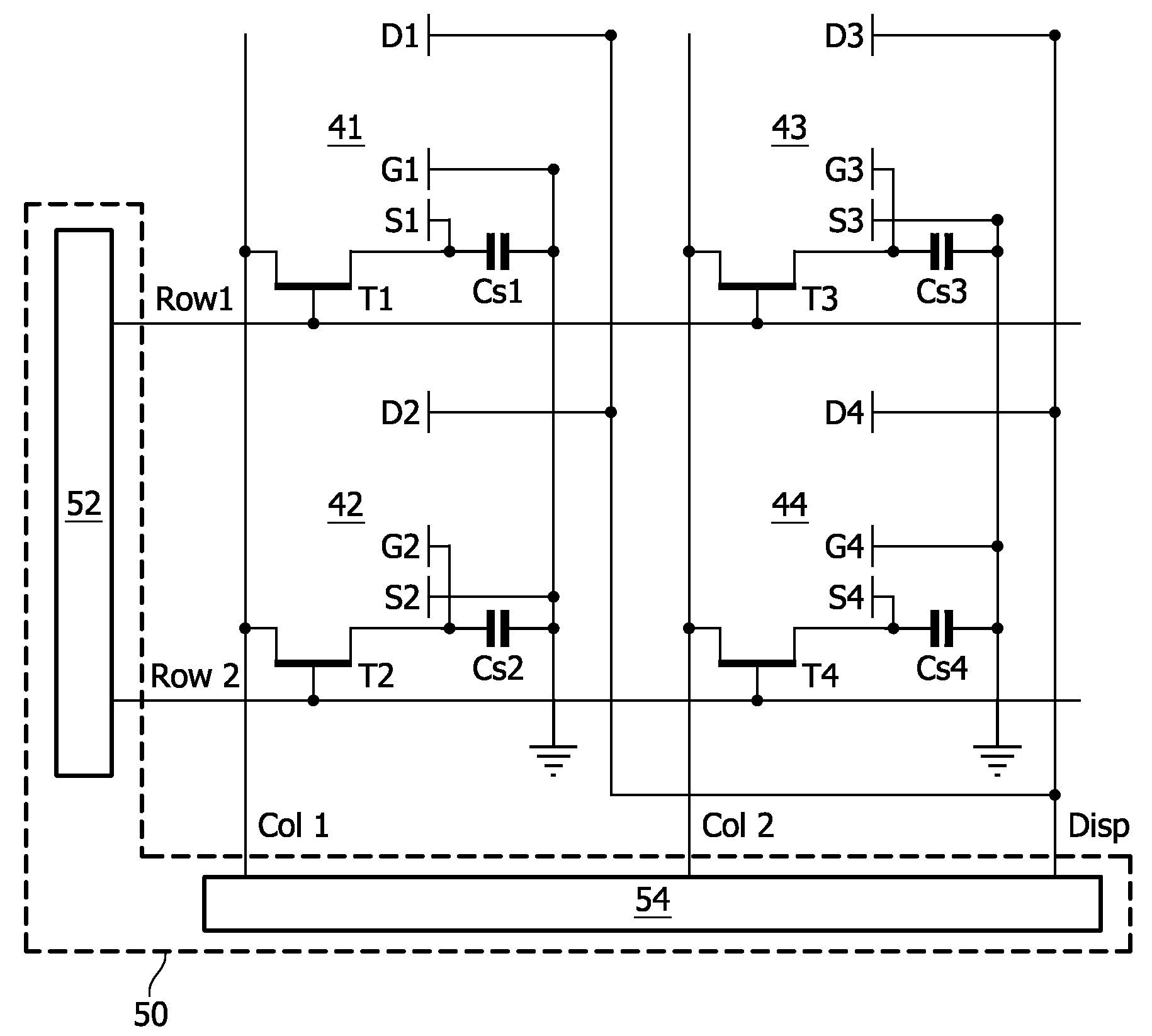
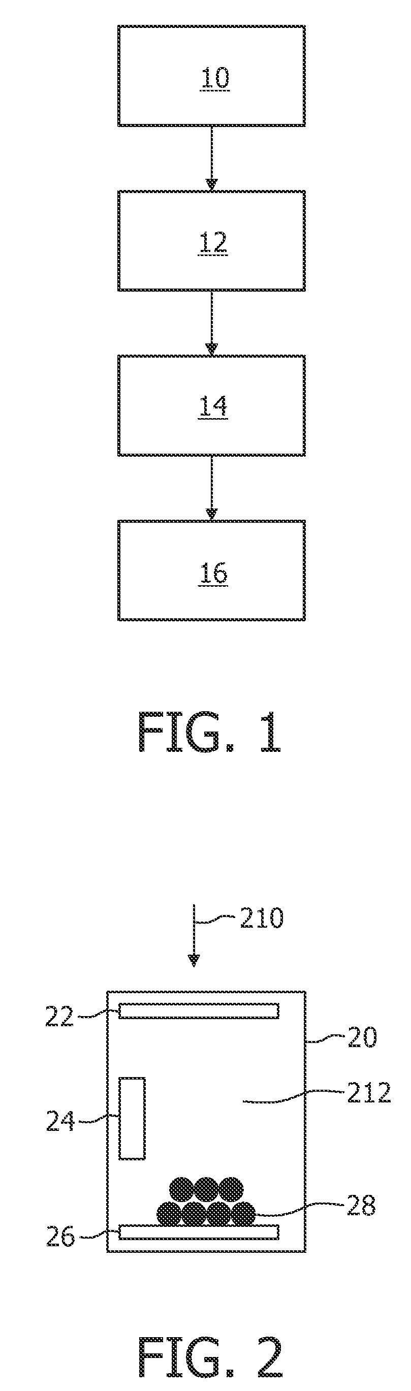
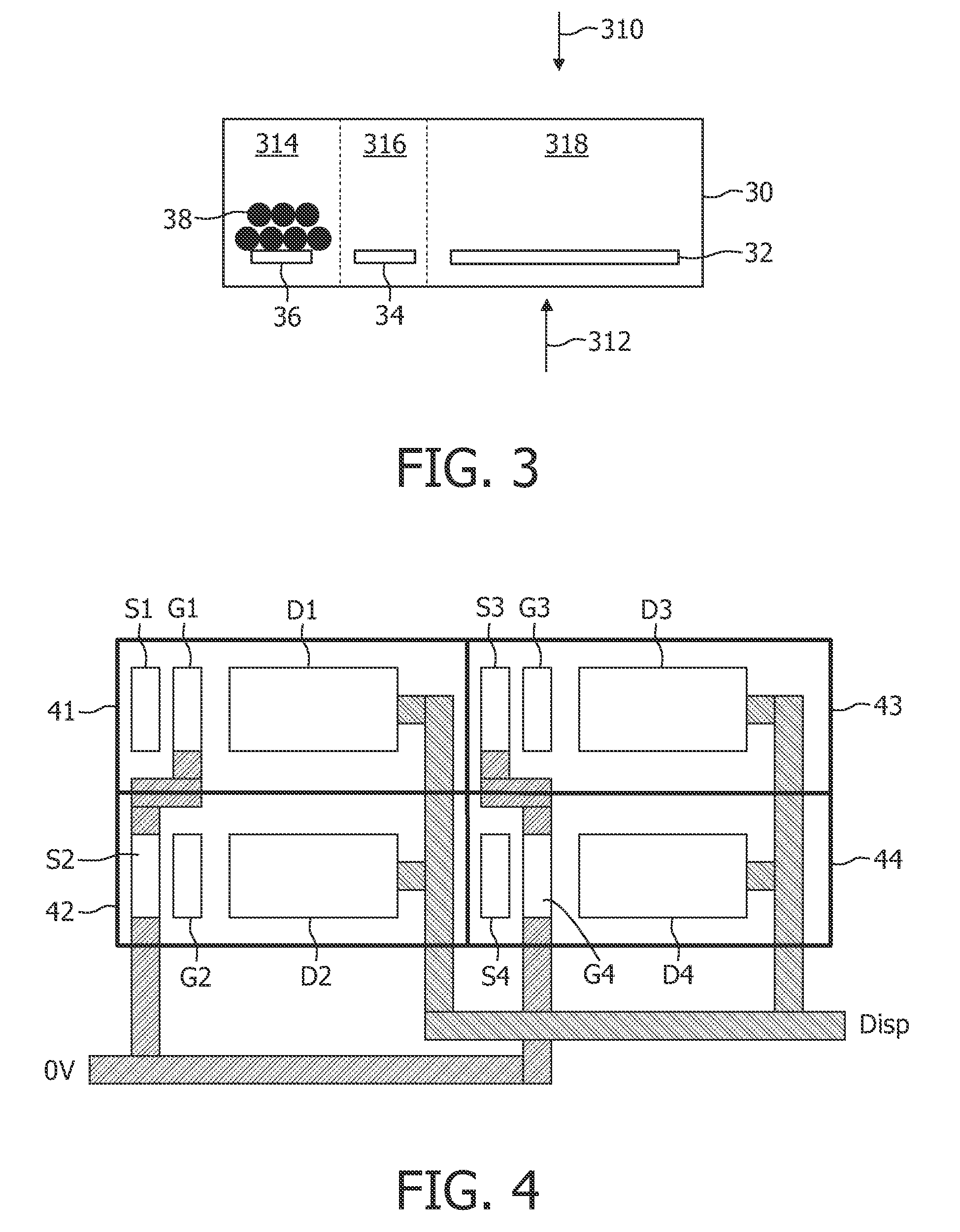
[0039]FIG. 1 shows a flow diagram of a method for driving a moving particle display device, which can be used for the display device of the invention. The moving particle display device typically has hundreds or thousands of moving particle cells, each of which form a first or second cell of a pair. Each cell comprises movable charged particles, and has a storage region into which at least some of the movable charged particles may be moved, a gate region into which at least some of the movable charged particles may be moved, and a display region into which at least some of the movable charged particles may be moved.

[0040]A cell's display region is the region of the cell that determines the cell's optical state. The optical state is determined by the number of (movable charged) particles that are within the cell's display region. The cell's gate region is a region of the cell from which particles are moved into the display region. The cell's storage region is a region where the cell'...


PUM

PropertyMeasurementUnit
transparentaaaaaaaaaa
voltageaaaaaaaaaa

Abstract

A moving particle display device comprises an array of rows and columns of display pixels (41,42,43,44), a plurality of row address lines (Row1,Row2;72; 112), each row address line for addressing a respective row of pixels and a plurality of column address lines (Col1,Col2;76; 108), each for providing pixel data to a respective column of pixels. A plurality of discharge column lines (82) is provided. A pixel is addressed by addressing a row of pixels and providing data to the pixels in the addressed row using the column address lines (Col1,Col2;76; 108). A charge flow from a column address line to an addressed pixel in the column flows to a respective discharge column line (82). By having discharge lines in the column direction, when a row of pixels is addressed, a current flow through the pixel, which is used to load data into the pixel from a column address line, passes to a column discharge line. In this way, the column discharge line only carries a current flow associated with a small number of pixels from the row. This enables the width of the discharge lines to be kept to a minimum, and it also enables the number of pixels in a row to be scaled without requiring the discharge line to carry an increased current.

Description

FIELD OF THE INVENTION[0001]The invention relates to a moving particle display device, and in particular to a pixel electrode layout for such a display.BACKGROUND OF THE INVENTION[0002]Previous moving particle displays, such as electrophoretic displays, have been known for many years; for example from U.S. Pat. No. 3,612,758.[0003]The fundamental principle of electrophoretic displays is that the appearance of an electrophoretic material encapsulated in the display is controllable by means of electrical fields.[0004]To this end the electrophoretic material typically comprises electrically charged particles having a first optical appearance (e.g. black) contained in a fluid such as liquid or air having a second optical appearance (e.g. white), different from the first optical appearance. The display typically comprises a plurality of pixels, each pixel being separately controllable by means of separate electric fields supplied by electrode arrangements. The particles are thus movable ...

Claims


Application Information

Patent Timeline
Patent Type & Authority Applications(United States)
IPC IPC(8): G09G3/34G02F1/167G02F1/16766
CPCG02F1/134363G02F1/167G02F2001/1676G09G2320/0233G09G2300/0426G09G2300/0434G09G2300/08G09G3/3446G02F1/16766H04L1/1825H04L1/1864H04L1/1896H04L1/20H04L5/006
Inventor DEANE, STEVEN CHARLESFRENCH, IAN
Owner ADREA LLC
Why Eureka
Try Eureka