Seven transistor SRAM cell

Inactive Publication Date: 2009-06-25
TEXAS INSTR INC
View PDF18 Cites 46 Cited by
  • Summary
  • Abstract
  • Description
  • Claims
  • Application Information

AI Technical Summary

Benefits of technology

[0007]Embodiments of the present disclosure provide a seven transistor static random access memory (7T SRAM) cell, a method of operating the 7T SRAM cell and an integrated circuit employing the 7T SRAM cell. In one embodiment, the 7T SRAM cell includes a pair of cross-coupled inverters configured to provide a memory element having first and second storage nodes. The 7T SRAM cell also includes a Read isolation transistor having a control element connected to one of the storage nodes of the cross-coupled transistor inverters and configured to provide a buffered Read output from the memory element. The 7T SRAM cell further includes a Read pass gate transistor controlled by a Read word line and connected between the Read isolation transistor and a read bit line to read the buffered Read output. Additionally, the 7T SRAM cell still further includes a Write pass gate transistor controlled by a Write word line and connected between one of the storage nodes of the cross-coupled inverters and a Write bit line to write either state of the memory element.
[0008]The present disclosure also provides, in another aspect, a method of operating a 7T SRAM cell. The method includes providing a memory element with a pair of cross-coupled inverters having first and second storage nodes. The method also includes writing a memory state of the memory element from a Write bit line to one of the first and second storage nodes through

Problems solved by technology

Inappropriate transistor parameter values in conjunction with the BL and WL voltages applied during a READ may result in an unwanted change in state of the memory cell due to random asymmetries caused by imperfections in the manufacturing process.
The necessity to guard against such READ instability places an undesirable constraint on the design parameters of the transistors in the 6T SRAM cell.
This constraint limits the ability of a designer to increase READ performance of th

Method used


Image

  • Seven transistor SRAM cell
  • Seven transistor SRAM cell
  • Seven transistor SRAM cell

Examples


Embodiment Construction

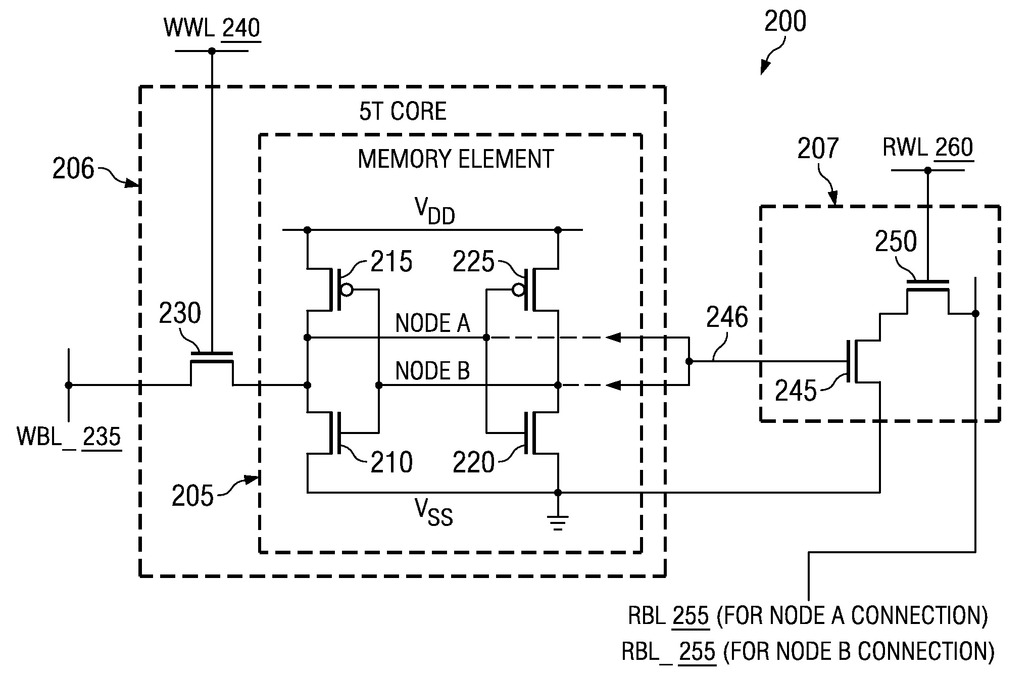
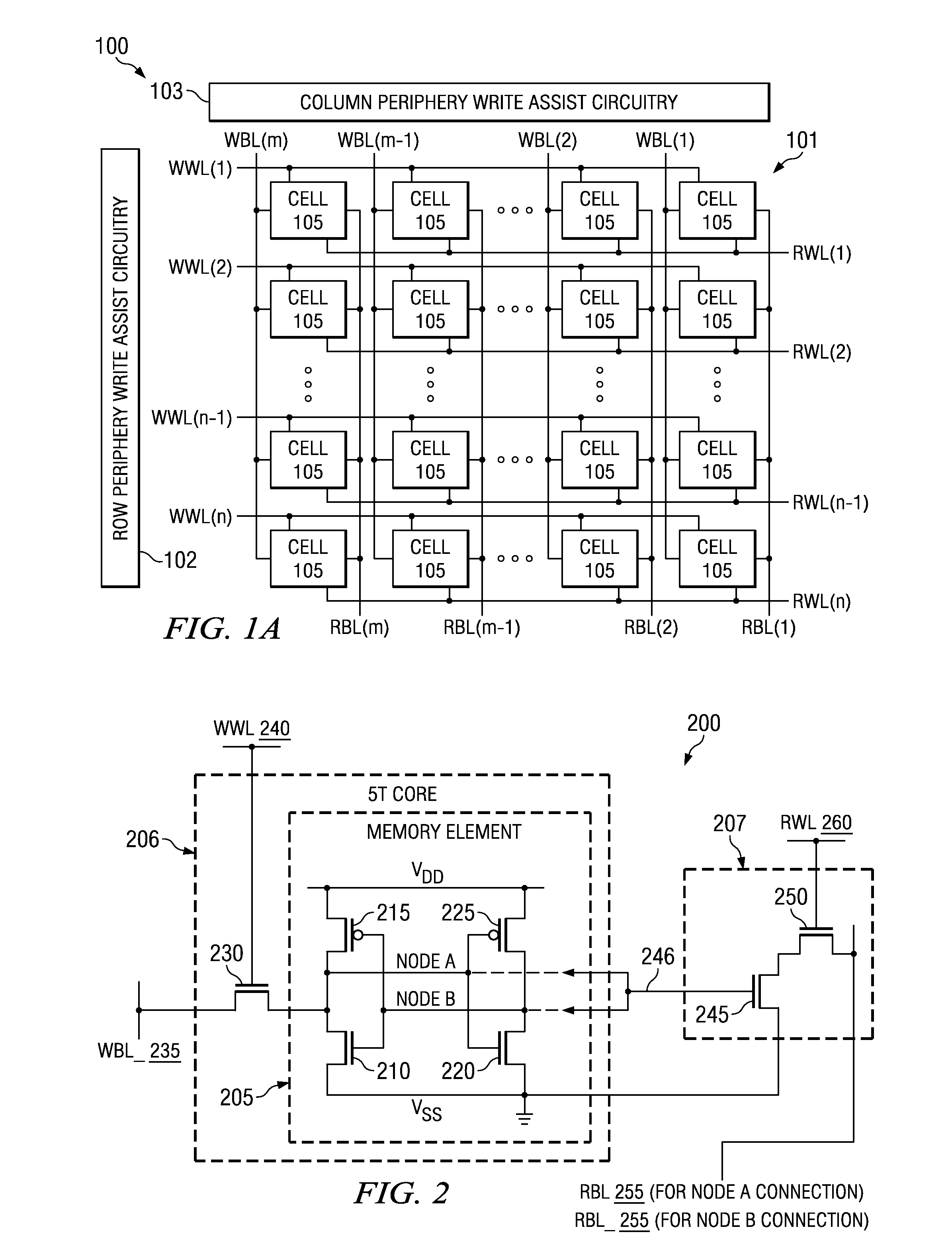
[0025]The present disclosure provides embodiments of a 7T SRAM cell that may be employed to mitigate at least a portion of the problems associated with scaling to smaller geometries. The 7T SRAM cell employs a single-sided WRITE and a single-sided READ, wherein the single sided READ uses a gain cell type output. In addition to providing a smaller footprint area than an 8T SRAM cell, this configuration maintains an adequate static noise margin (SNM) as well as provides robustness for WRITE (Vtrip), good read current capabilities (Iread) and low leakage current (IDDQ).

[0026]FIG. 1A illustrates an integrated circuit 100 including an SRAM array 101 as provided by one embodiment of the disclosure. The SRAM array 101 is shown having memory cells 105 wherein each cell is a 7T SRAM cell employing single and separate Write and Read word lines as well as single and separate Write and Read bit lines. The SRAM array 101 includes a plurality of Write word lines WWL(1)-WWL(n) and corresponding Re...


PUM


Abstract

The present disclosure provides a seven transistor static random access memory (7T SRAM) cell. In one embodiment, the 7T SRAM cell includes a pair of cross-coupled inverters configured to provide a memory element having first and second storage nodes. The 7T SRAM cell also includes a Read isolation transistor having a control element connected to one of the storage nodes of the cross-coupled transistor inverters and configured to provide a buffered Read output. The 7T SRAM cell further includes a Read pass gate transistor controlled by a Read word line and connected between the Read isolation transistor and a read bit line. Additionally, the 7T SRAM cell still further includes a Write pass gate transistor controlled by a Write word line and connected between one of the storage nodes of the cross-coupled inverters and a Write bit line to write either state of the memory element.

Description

TECHNICAL FIELD OF THE INVENTION[0001]The present invention is directed, in general, to a static random access memory (SRAM) and, more specifically, to a seven transistor SRAM employing both single-sided writing and buffered, single-sided reading capabilities.BACKGROUND OF THE INVENTION[0002]A typical SRAM device is designed to store many thousands of bits of information. These bits are stored in individual cells, organized as rows and columns to make efficient use of space on a semiconductor substrate containing the SRAM device. A commonly used cell architecture is known as the “6T” cell, by virtue of having six MOS transistors. Four transistors defining an SRAM cell core or memory element are configured as cross-coupled CMOS inverters, which act as a bistable circuit that indefinitely holds the state imposed onto it while powered. Each CMOS inverter includes a load or “pull-up” transistor and a driver or “pull-down” transistor. The output of the two inverters will be in opposite s...

Claims


Application Information

Patent Timeline
IPC IPC(8): G11C11/00G11C7/00
CPCG11C11/412
Inventor HOUSTON, THEODORE W.
Owner TEXAS INSTR INC
Why Eureka
Try Eureka