
Magnetic random access memory with write and read circuits using magnetic tunnel junction (MTJ) devices

Inactive Publication Date: 2002-11-12
SAMSUNG ELECTRONICS CO LTD
View PDF3 Cites 25 Cited by
  • Summary
  • Abstract
  • Description
  • Claims
  • Application Information

AI Technical Summary

Benefits of technology

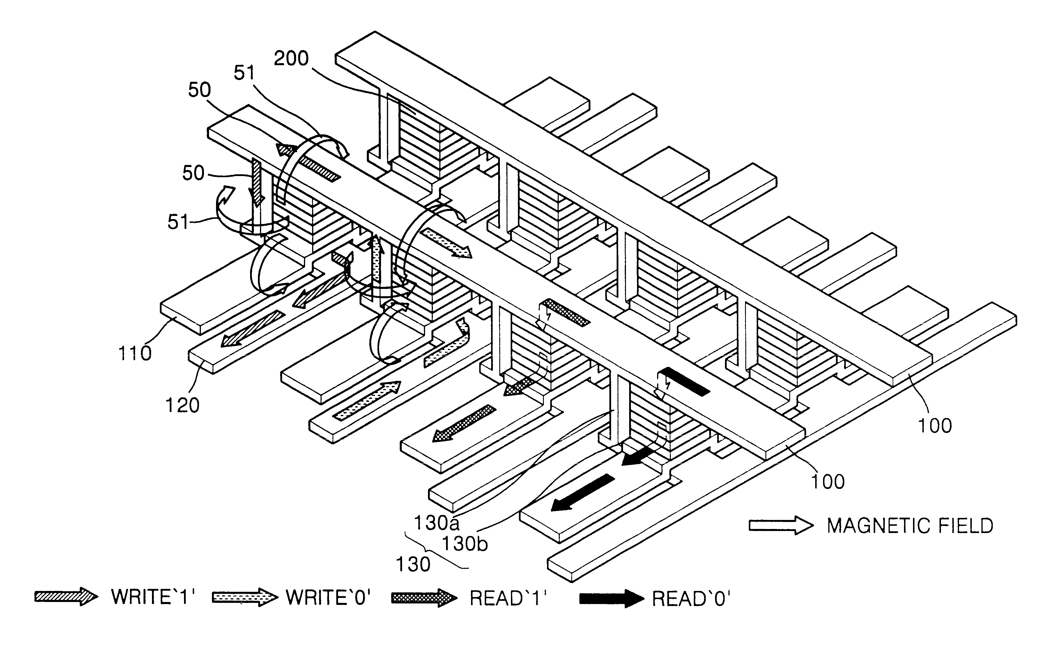
As described above, MTJs are disposed at each intersection region of the word and bit lines to form memory cells. The memory cells are formed to apply an electric field having enough strength to change the magnetization direction of the MTJs only to selected cells. A write bit line is formed additionally to a read bit line to allow current to bypass each selected MTJ to flow through the write bit line in a write operation, so that the magnetization direction of the free ferromagnetic layer in an MTJ is parallel or antiparallel to the fixed magnetization direction of the pinned ferromagnetic layer by the current flowing through a word line and a current bypass path. Thus, such bypass current can increase the intensity of a magnetic field, which in turn affects an MTJ. Further, this architecture enables a magnetic memory to random access a cross point in both read and write operations.

Problems solved by technology

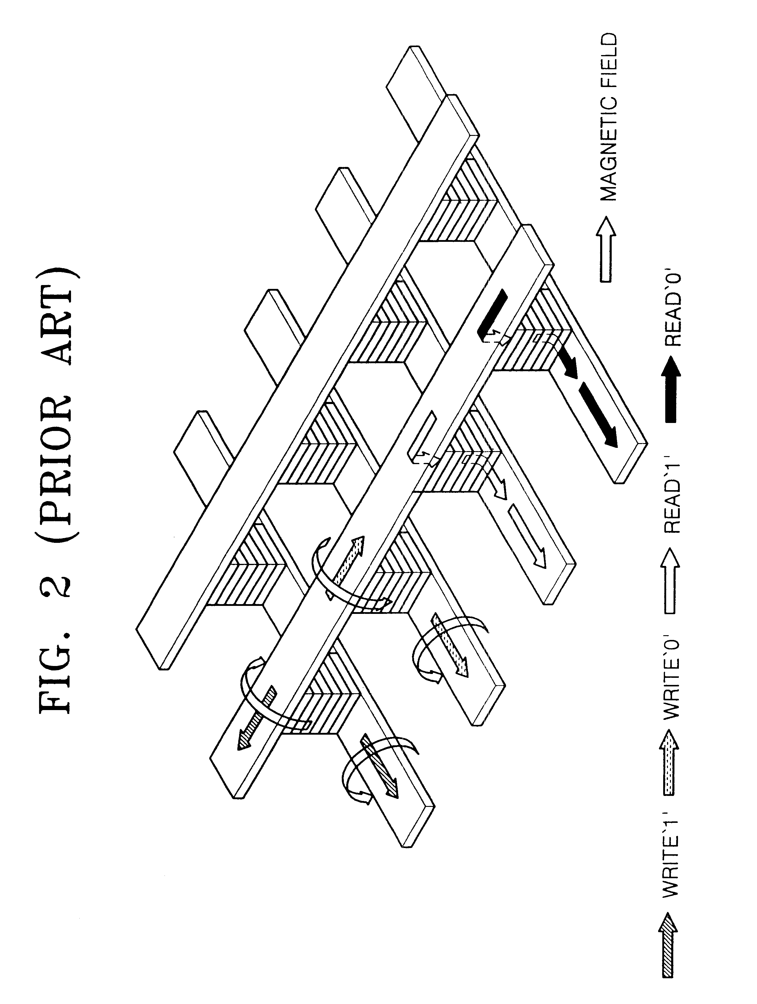
Accordingly, this conventional device has a problem in that the direction of a magnetic field created in the MTJ of FIG. 3A is not formed in parallel or antiparallel to the fixed magnetization of a pinned ferromagnetic layer, as illustrated in FIGS. 3B and 3C.

Method used


Image

  • Magnetic random access memory with write and read circuits using magnetic tunnel junction (MTJ) devices
  • Magnetic random access memory with write and read circuits using magnetic tunnel junction (MTJ) devices
  • Magnetic random access memory with write and read circuits using magnetic tunnel junction (MTJ) devices

Examples


Embodiment Construction

Korean patent application number 00-5489, filed Feb. 3, 2000, and entitled: "Magnetic Random Access Memory with Write and Read Circuits Using Magnetic Tunnel Junction (MTJ) Devices," is incorporated by reference herein in its entirety. A preferred embodiment will now be described in detail with reference to the accompanying figures.

A magnetic random access memory according to the present invention includes read and write circuits for reading and writing the magnetic state of a free ferromagnetic layer, using magnetic tunnel junction (MTJ) devices. More specifically, the subject matter of the present invention provides an architecture which enables the magnetic memory to change the magnetization direction of a free ferromagnetic layer effectively by altering the structure of a write circuit of an MTJ formed at the cross point of word and bit lines, and has random access to the cross point of the two lines.

Referring to FIG. 4, which is a perspective view illustrating the structure of ...


PUM


Abstract

A magnetic random access memory with write and read circuits using magnetic tunnel junction (MTJ) devices wherein MTJs are arranged at cross points of word lines and read bit lines to form memory cells. After write bit lines and read bit lines are arranged parallel to each other, current bypass paths are formed allowing current to bypass the side and bottom of the MTJ. Thus, an electric field having intensity enough to change the magnetization direction of the MTJ, is applied only to each selected cell. In a write operation, the magnetization direction of a free layer in the MTJ is formed to be parallel or antiparallel to the magnetization direction of a pinned ferromagnetic layer by the current passing through the word line and the current bypass path.

Description

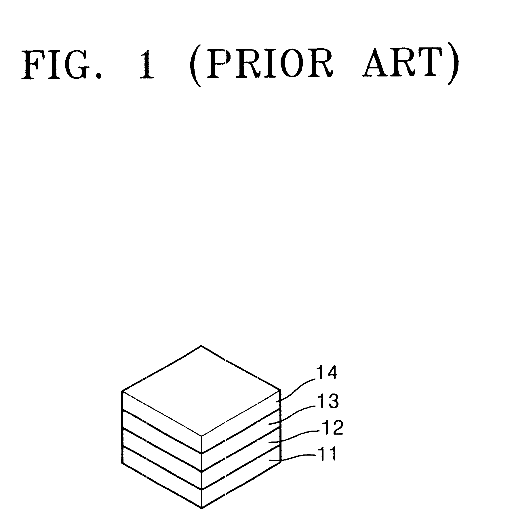
1. Field of the InventionThe present invention relates to a nonvolatile memory device. More specifically, the present invention relates to a magnetic random access memory with write and read circuits using magnetic tunnel junction (MTJ) devices.2. Description of the Related ArtA nonvolatile magnetic random access memory is an array of individual magnetic memory cells. Each memory cell includes a magnetic tunnel junction (MTJ) device. FIG. 1 illustrates the basic structure of a MTJ device in a conventional magnetic memory cell. Referring initially to FIG. 1, each MTJ device includes a pinned ferromagnetic layer 12, the magnetization direction of which is fixed, an antiferromagnetic layer 11, for pinning the magnetization of the pinned ferromagnetic layer 12 by use of an antiferromagnetic coupling, a free ferromagnetic layer 14, the magnetization direction of which is free to rotate parallel or antiparallel to the fixed magnetization direction of the pinned ferromagnetic layer 12, and...

Claims


Application Information

Patent Timeline
Patent Type & Authority Patents(United States)
IPC IPC(8): G11C11/15G11C11/02H01L21/8246H01L27/105H01L43/08G11C11/14
CPCG11C11/15G11C11/02
Inventor PARK, SANG-JINSOK, JUNG-HYUNCHUNG, IL-SUB
Owner SAMSUNG ELECTRONICS CO LTD
Learn More