Circuit substrate, circuit device and manufacturing process thereof

a technology of circuit substrate and substrate, which is applied in the direction of printed circuit aspects, printed circuit non-printed electric components association, conductive pattern formation, etc., can solve the problems of large substrate b>100/b> dimension, difficult to downsize the entire device, and difficult to achieve the structure of the substrate b>100/b>

Active Publication Date: 2009-07-02
SEMICON COMPONENTS IND LLC
View PDF4 Cites 31 Cited by
  • Summary
  • Abstract
  • Description
  • Claims
  • Application Information

AI Technical Summary

Benefits of technology

[0028]The invention further provides a semiconductor device that includes a metal substrate including a top surface, a bottom surface and four side surfaces, the top surface being insulated, a conductive pattern insulated from the metal substrate, and a semiconductor element mounted on and electrically connected to the conductive pattern. Each of the side surfaces of the metal substrate includes a first inclining side surface and a second inclining side surface so as to form a convex shape protruding outwardly between the top surface and the bottom surface of the metal substrate, and the first inclining side surfaces of a pair of two opposing side surfaces are smaller than corresponding first inclining side surfaces of another pair of two opposing side surfaces.

Problems solved by technology

However, there was the problem that it is difficult for the structure of the substrate 100 shown in FIG. 11(A) to achieve both high-voltage and downsizing.
In addition, because the first side surface 118 and the second side surface 120 are inclined equally and protrude outside, the dimension of the substrate 100 becomes large and the downsizing of the entire device becomes difficult.
This metallic burr would be removed by means of spraying vapor or liquid in high pressure, however, it is difficult to remove all of the metallic burr.

Method used


Image

  • Circuit substrate, circuit device and manufacturing process thereof
  • Circuit substrate, circuit device and manufacturing process thereof
  • Circuit substrate, circuit device and manufacturing process thereof

Examples


first embodiment

The First Embodiment

Structure of a Circuit Substrate and a Circuit Device

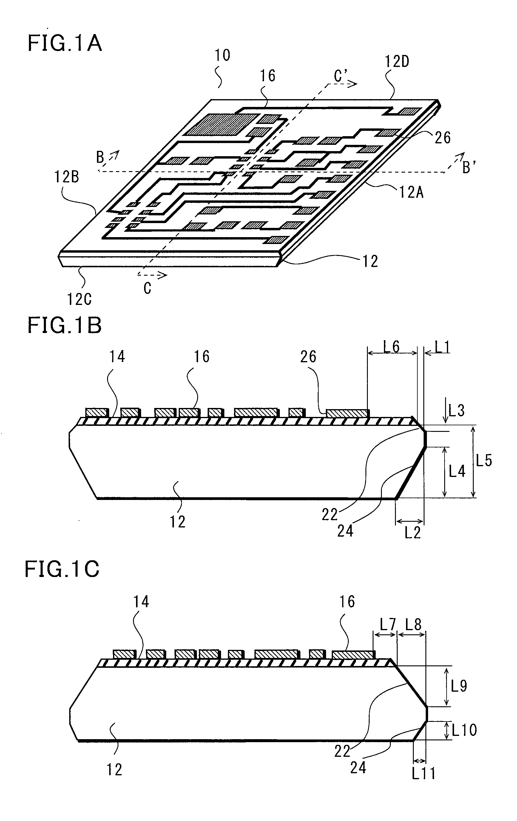
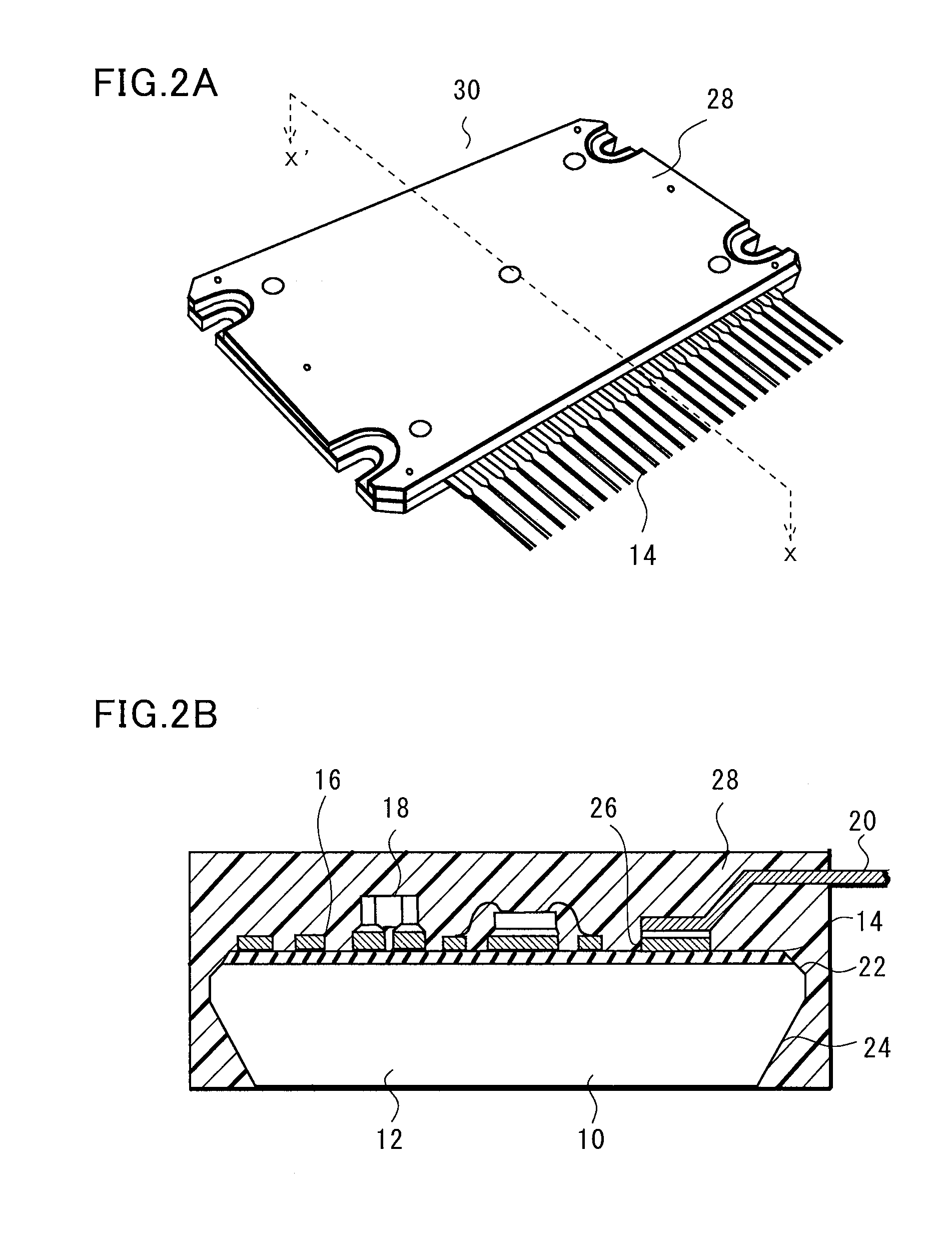
[0041]Referring to FIG. 1, it explains the structure of a circuit substrate 10 which embodies this invention. FIG. 1(A) is a oblique view of the circuit substrate 10 seen from the upper side, FIG. 1 (B) is the cross section view at the line between B and B′ in FIG. 1(A), and FIG. 1(C) is the cross section view at the line between C and C′ in FIG. 1(A).

[0042]Referring to FIG. 1, the circuit substrate 10 consists of metal substrate 12, an insulating layer covering the top surface of the metal substrate 12, and a conductive pattern 16 formed on the top surface of the insulating layer 14.

[0043]The metal substrate 12 is a substrate which consists of metal that is mainly made of aluminum or cupper, etc., and the size of dimension is, for example, about 1 cm×2 cm, The thickness of the metal substrate 12 is, for example, 1.5 mm. When the metal substrate 12 consists of aluminum, the top and bottom surfaces are covered b...

second embodiment

The Second Embodiment

Manufacturing Method for Circuit Substrates and Circuit Devices

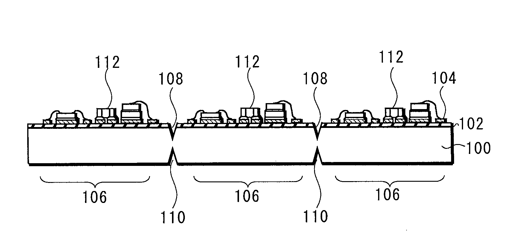
[0067]In this embodiment, referring to FIG. 4 and followings, it explains manufacturing method for circuit substrates and circuit devices.

[0068]Referring to FIG. 4, first of all, the groove which has a shape of V-type in cross section is formed on the both top and bottom surface of a large scale substrate 50. Referring to FIG. 4 (A), the substrate 50 is a large size substrate on which a lot of circuit substrates are able to be formed and the dicing line is provided in a grid according to the size of the circuit substrate formed thereon. Here, dicing line D1 is provided in a lateral direction and dicing line D2 is provided in a longitudinal direction. Resin material such as glass epoxy, etc. and ceramic may be adopted as material of the substrate 50 though the substrate that consists of metal such as aluminum, etc. is adopted as the substrate 50 here.

[0069]Referring to FIG. 4 (B), a groove which has V...


PUM

PropertyMeasurementUnit
thicknessaaaaaaaaaa
thicknessaaaaaaaaaa
widthaaaaaaaaaa

Abstract

A semiconductor device that includes a metal substrate including a top surface, a bottom surface and four side surfaces, a conductive pattern insulated from the metal substrate, and a semiconductor element mounted on and electrically connected to the conductive pattern. The top surface is insulated. Each of the side surfaces of the metal substrate includes a first inclining side surface and a second inclining side surface so as to form a convex shape protruding outwardly between the top surface and the bottom surface of the metal substrate, and the first inclining side surfaces of a pair of two opposing side surfaces are smaller than corresponding first inclining side surfaces of another pair of two opposing side surfaces.

Description

[0001]This application claims priority from Japanese Patent Application No. 2007-334237, the content of which is incorporated herein by reference in its entirety.BACKGROUND OF THE INVENTION[0002]1. Field of the Invention[0003]This invention relates to a circuit substrate and a circuit device and manufacturing process therefor. Especially, this invention relates to a circuit substrate and a circuit device on which plurality of circuit elements are mounted, and manufacturing process thereof.[0004]2. Description of the Related Art[0005]Previously, such method of separating each unit has been adopted: a conductive pattern which consists of a lot of units is formed on one large substrate, this conductive pattern is connected to circuit elements and, after that, each unit is separated (refer to the following patent document 1).[0006]Referring to FIG. 10, previous circuit substrates and manufacturing method thereof will be described. FIG. 10(A), FIG. 10(B) and FIG. 10(C) are cross section ...

Claims


Application Information

Patent Timeline
Patent Type & Authority Applications(United States)
IPC IPC(8): H01L23/48H01L21/768
CPCH05K1/05H01L2224/48227H05K3/0052H05K3/284H05K3/44H05K2201/09036H05K2201/0909H05K2201/09154H05K2201/09745H05K2203/1572H05K1/056H01L2224/32225H01L24/97H01L2224/73265Y10T29/49155H01L2924/19105H01L2224/97H01L2924/00012H01L2224/83H01L2224/85H01L2924/00H01L24/73H01L2924/14H05K1/02H05K1/18
Inventor NOGUCHI, MITSURUTAKAKUSAKI, SADAMICHI
Owner SEMICON COMPONENTS IND LLC
Why Eureka
Try Eureka