
Step-down circuit, semiconductor device, and step-down circuit controlling method
- Summary
- Abstract
- Description
- Claims
- Application Information
AI Technical Summary
Benefits of technology
Problems solved by technology
Method used
Image

Examples
first exemplary embodiment
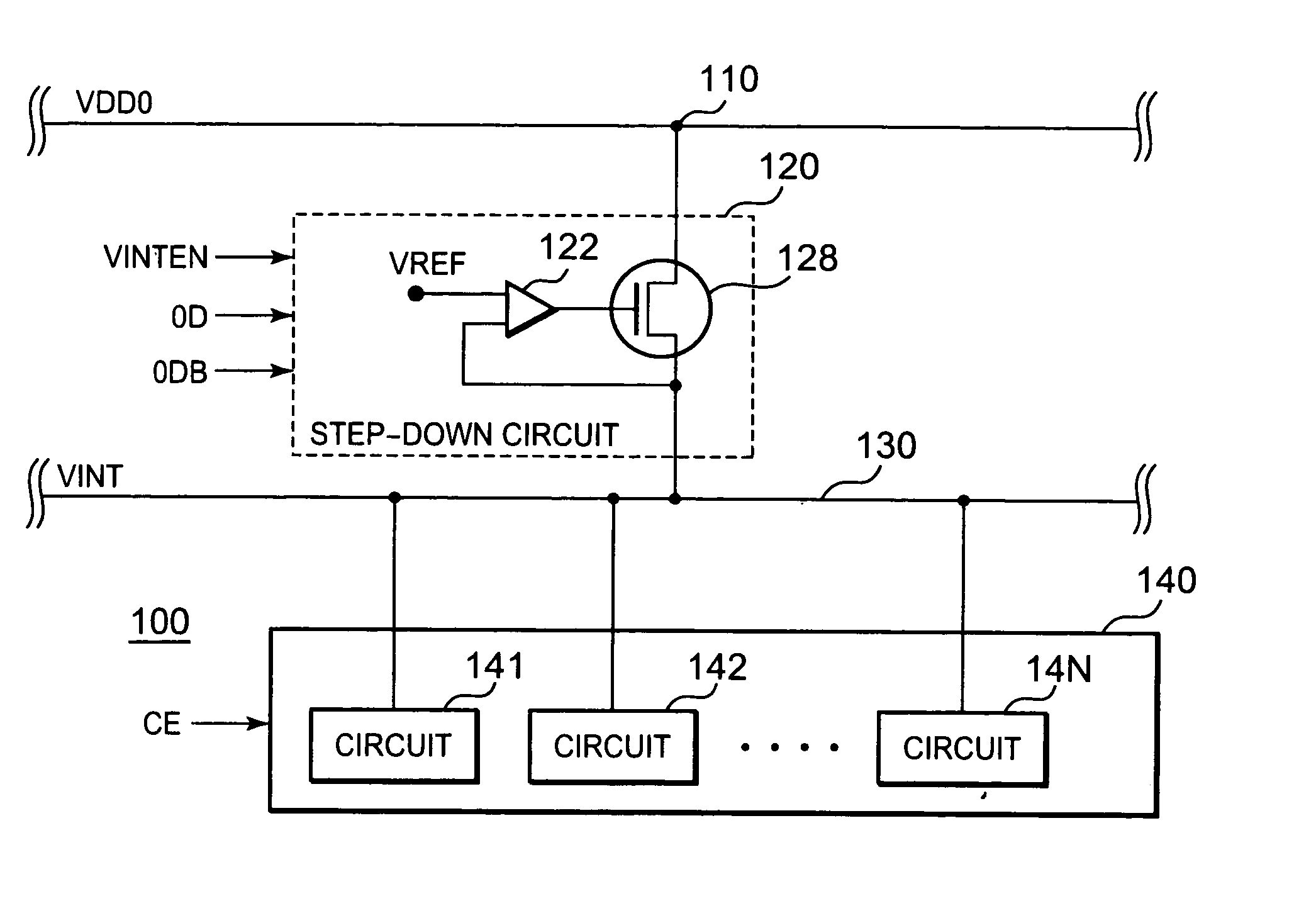
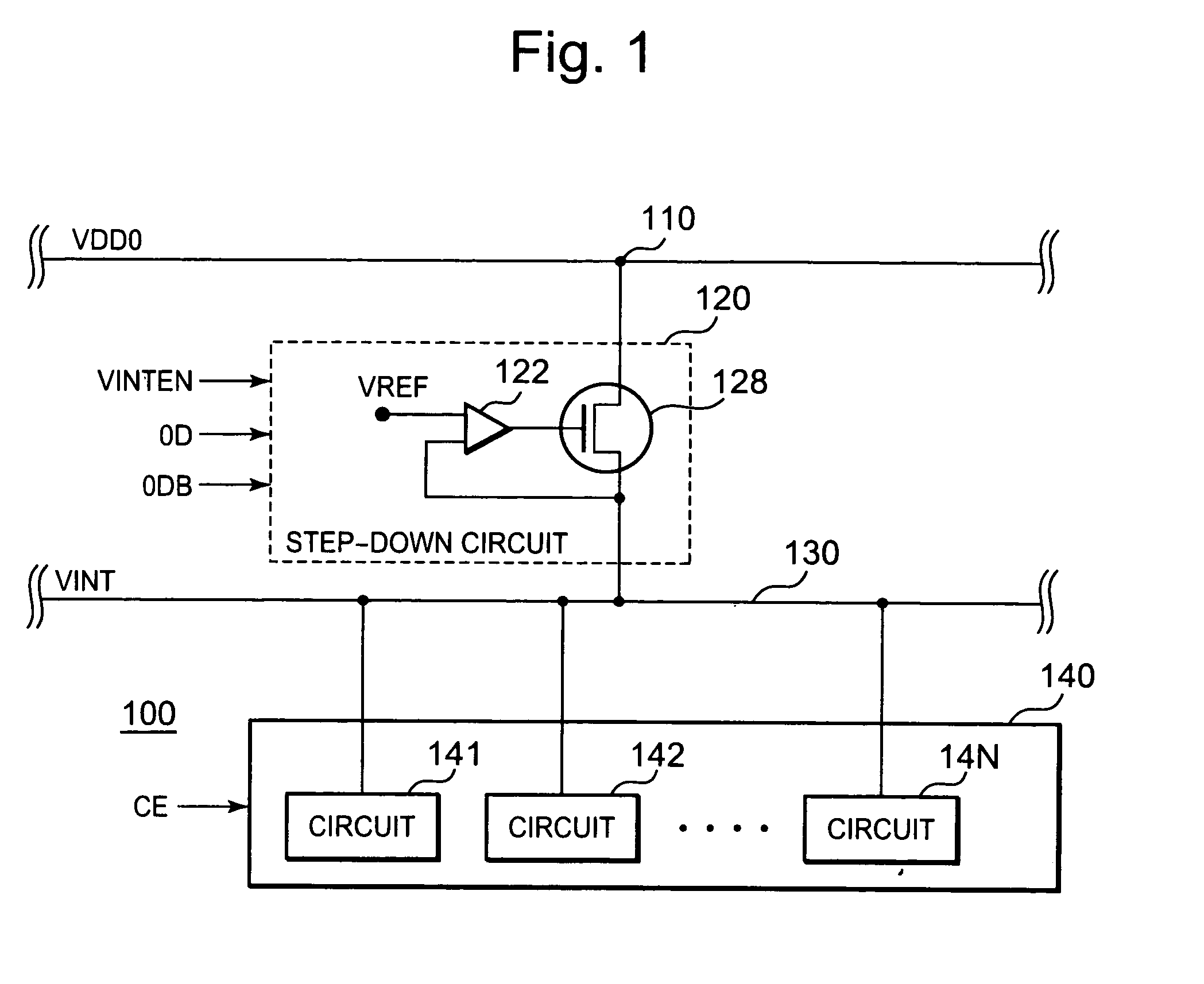
[0056]FIG. 1 shows a semiconductor device 100 in this first exemplary embodiment of the present invention. The semiconductor device 100 includes a circuit group 140 and a step-down circuit 120 that steps down a system supply voltage 140, which is an external supply voltage, and supplies the stepped-down voltage to the circuit group 140. The step-down circuit 120 is connected between a power supply node 110 and an internal power supply line 130, as well as a comparison circuit 122 and a driver 128.
[0057]The circuit group 140 includes plural circuits and is activated synchronously with a circuit activation enable signal CE that is turned on in a standby period in which the circuit 140 is idle, then the circuit group 140 enters an active period. Then, synchronously with the circuit activation enable signal CE that is turned off in the active period, the circuit group 140 is deactivated and enters another standby period. The operation voltage of the circuit group 140 is premised to be V...
second exemplary embodiment
[0086]The semiconductor device 100 in the above first exemplary embodiment is provided with one step-down circuit 120 with respect to the circuit group 140. The technique of this second exemplary embodiment can also apply to a semiconductor device provided with plural step-down circuits.
[0087]FIG. 4 shows a semiconductor device 200 in this second exemplary embodiment. In FIG. 4, the same reference numerals are used for the same functional components as those of the semiconductor device 100 shown in FIG. 1, avoiding redundant description.
[0088]As shown in FIG. 4, in the semiconductor device 200, plural step-down circuits 120 (two circuits in FIG. 4) are provided in parallel with respect to the circuit group 140. Those step-down circuits 120 are equivalent to the step-down circuit 120 provided in the semiconductor device 100 shown in FIG. 1 respectively, so the description for them will be omitted here.
[0089]The technique of the present invention can also apply to a case in which plur...
third exemplary embodiment
[0090]FIG. 5 shows a semiconductor device 300 in this third exemplary embodiment of the present invention. The semiconductor device 300 is also realized by applying the technique of the present invention to a semiconductor device provided with plural step-down circuits. In FIG. 5, the same reference numerals are used for the same functional components as those of the semiconductor device 200 shown in FIG. 4, avoiding redundant description.
[0091]As shown in FIG. 5, in the semiconductor device 300, plural step-down circuits 140 (two circuits in FIG. 5) are provided in parallel with respect to a circuit group 140. Those two step-down circuits are the step-down circuits 320 and 120. Among the circuits included in the circuit group 140, the circuit 14N is high in current consumption.
[0092]The step-down circuit 120 is configured so as to carry out both overdriving and overdriving backward (e.g., reversely). The step-down circuit 320 is a conventional one that does not carry out any of the...
PUM
 Abstract
Description
Claims
Application Information