Step-down circuit, semiconductor device, and step-down circuit controlling method

a technology of step-down circuit and control method, which is applied in the direction of digital storage, electrical pulse generator details, instruments, etc., can solve the problems of unstable operation of circuit group b>10/b>, excessive charge supply, and overdriving, so as to achieve favorable power supply responsibility

Inactive Publication Date: 2010-11-23
RENESAS ELECTRONICS CORP
View PDF5 Cites 20 Cited by
  • Summary
  • Abstract
  • Description
  • Claims
  • Application Information

AI Technical Summary

Benefits of technology

[0021]Overdriving to be carried out to prevent the over-drop as described above makes it possible to improve the power supply responsibility at the activation of the object circuit and shorten the step-down circuit response period A2, thereby shortening the restoration period A3. On the other hand, such overdriving is also expected to worsen the power supply responsibility of the object circuit at the deactivation of the circuit.
[0027]According to the techniques of the present invention, it is possible to realize a favorable power supply responsibility even at the activation and deactivation timings of an object circuit upon supplying a stepped-down supply voltage to the object circuit.

Problems solved by technology

On the other hand, such overdriving is also expected to worsen the power supply responsibility of the object circuit at the deactivation of the circuit.
If overdriving is carried out in such a case, therefore, an excessive charge supply might occur.
Furthermore, the operation of the circuit group 10 might become unstable.
However, it is difficult to grasp the charge consumption of the peripheral logic in operation, since the current consumption is varied among operation patterns.

Method used


Image

  • Step-down circuit, semiconductor device, and step-down circuit controlling method
  • Step-down circuit, semiconductor device, and step-down circuit controlling method
  • Step-down circuit, semiconductor device, and step-down circuit controlling method

Examples


first exemplary embodiment

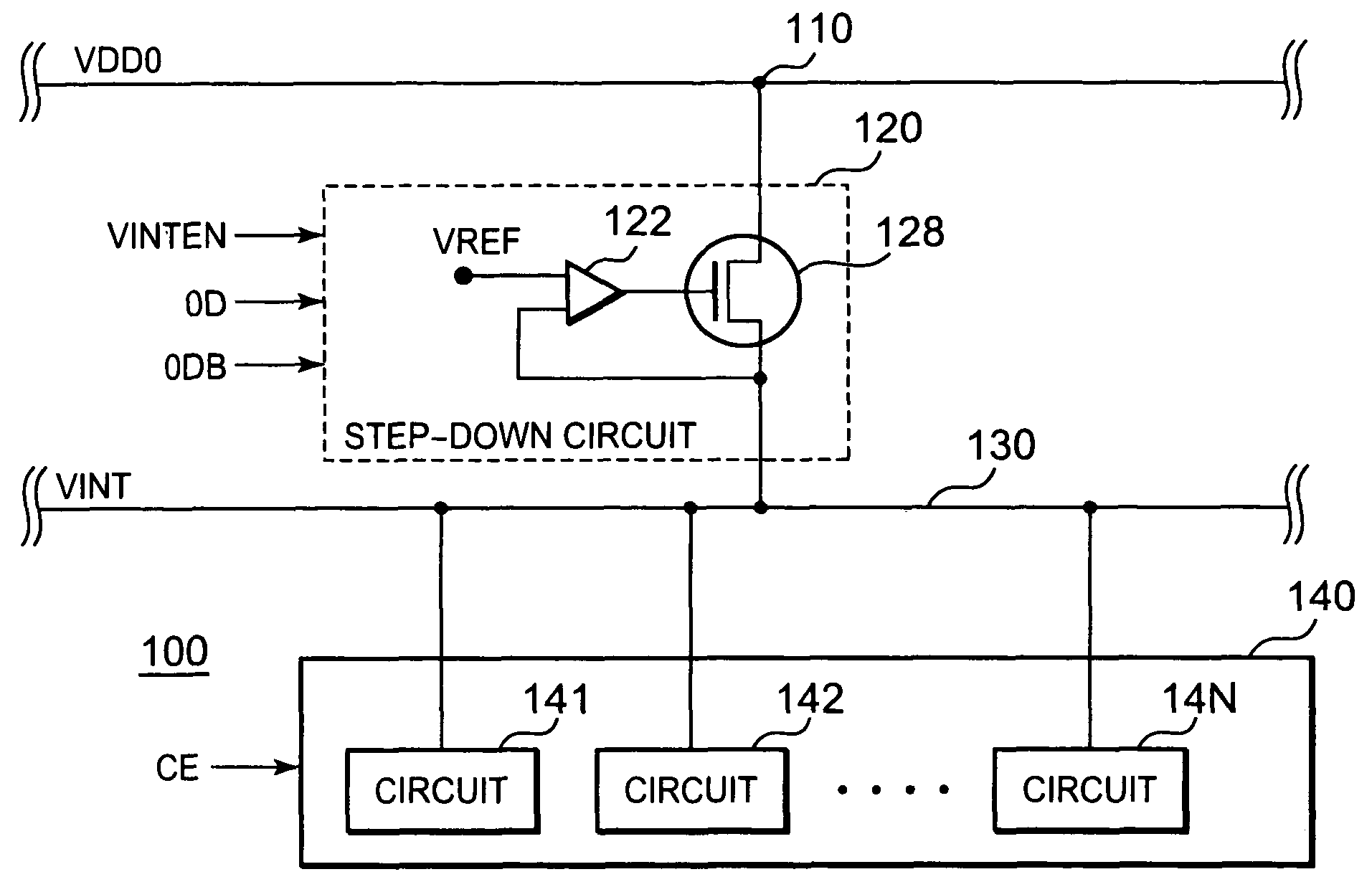
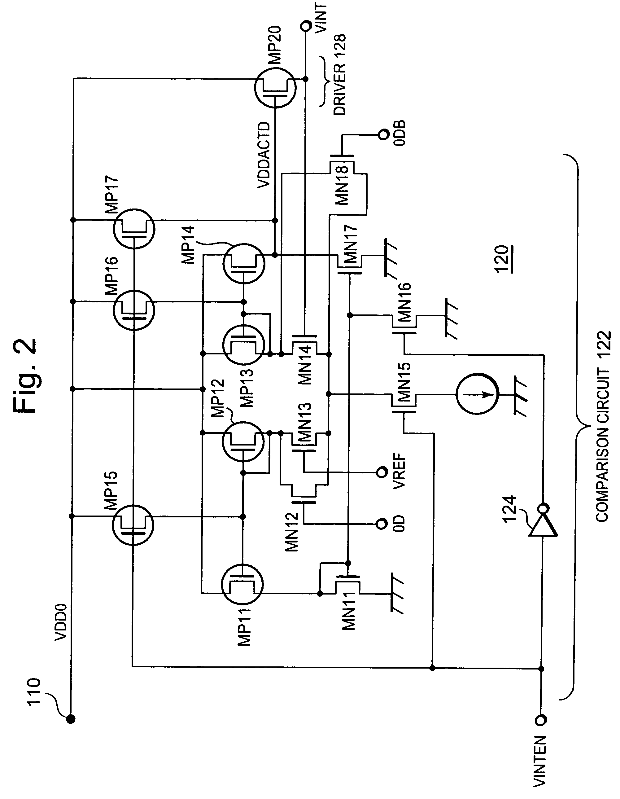
[0056]FIG. 1 shows a semiconductor device 100 in this first exemplary embodiment of the present invention. The semiconductor device 100 includes a circuit group 140 and a step-down circuit 120 that steps down a system supply voltage 140, which is an external supply voltage, and supplies the stepped-down voltage to the circuit group 140. The step-down circuit 120 is connected between a power supply node 110 and an internal power supply line 130, as well as a comparison circuit 122 and a driver 128.

[0057]The circuit group 140 includes plural circuits and is activated synchronously with a circuit activation enable signal CE that is turned on in a standby period in which the circuit 140 is idle, then the circuit group 140 enters an active period. Then, synchronously with the circuit activation enable signal CE that is turned off in the active period, the circuit group 140 is deactivated and enters another standby period. The operation voltage of the circuit group 140 is premised to be V...

second exemplary embodiment

[0086]The semiconductor device 100 in the above first exemplary embodiment is provided with one step-down circuit 120 with respect to the circuit group 140. The technique of this second exemplary embodiment can also apply to a semiconductor device provided with plural step-down circuits.

[0087]FIG. 4 shows a semiconductor device 200 in this second exemplary embodiment. In FIG. 4, the same reference numerals are used for the same functional components as those of the semiconductor device 100 shown in FIG. 1, avoiding redundant description.

[0088]As shown in FIG. 4, in the semiconductor device 200, plural step-down circuits 120 (two circuits in FIG. 4) are provided in parallel with respect to the circuit group 140. Those step-down circuits 120 are equivalent to the step-down circuit 120 provided in the semiconductor device 100 shown in FIG. 1 respectively, so the description for them will be omitted here.

[0089]The technique of the present invention can also apply to a case in which plur...

third exemplary embodiment

[0090]FIG. 5 shows a semiconductor device 300 in this third exemplary embodiment of the present invention. The semiconductor device 300 is also realized by applying the technique of the present invention to a semiconductor device provided with plural step-down circuits. In FIG. 5, the same reference numerals are used for the same functional components as those of the semiconductor device 200 shown in FIG. 4, avoiding redundant description.

[0091]As shown in FIG. 5, in the semiconductor device 300, plural step-down circuits 140 (two circuits in FIG. 5) are provided in parallel with respect to a circuit group 140. Those two step-down circuits are the step-down circuits 320 and 120. Among the circuits included in the circuit group 140, the circuit 14N is high in current consumption.

[0092]The step-down circuit 120 is configured so as to carry out both overdriving and overdriving backward (e.g., reversely). The step-down circuit 320 is a conventional one that does not carry out any of the...


PUM


Abstract

A step-down circuit is connected between a power supply node for supplying a supply voltage and an internal power supply line for supplying a power to the object circuit and steps-down the supply voltage, and supplies the stepped-down voltage to the object circuit through the internal power supply line. The step-down circuit includes a comparison circuit that compares a reference voltage with the voltage of the internal power supply line, and a driver that adjusts a current flowing between the internal power supply line and the power supply node according to the comparison result of the comparison circuit. The activity level of the driver is controlled so as to rise in a predetermined rising period synchronously with an activated operation of the object circuit and to fall in a predetermined falling period that comes after the rising period.

Description

BACKGROUND OF THE INVENTION[0001]1. Field of the Invention[0002]The present invention relates to a technique for stepping down a voltage, and more concretely to a technique for stepping down a supply voltage so as to be supplied to an object circuit.[0003]This application has foreign priority benefits of Japanese Patent Application No. 2007-336419 having a Japanese filing date of Dec. 27, 2007.[0004]2. Description of Related Art[0005]In case of each of processing systems provided with circuits that operate with a supply voltage that is lower than the system supply voltage, the system uses a step-down circuit to step down the system supply voltage to a supply voltage that operates those circuits. For example, in the fields of such semiconductor devices as the DRAM (Dynamic Random Access Memory and the pseudo SRAM (Static Random Access Memory), their elements are kept micronized more and more along with the progress of high density packing and highly integration techniques of LSIs. An...

Claims


Application Information

Patent Timeline
Patent Type & Authority Patents(United States)
IPC IPC(8): G05F1/10
CPCG05F1/56G11C5/147G11C11/406G11C11/40615G11C11/4074G11C2207/2227
Inventor HIROBE, ATSUNORI
Owner RENESAS ELECTRONICS CORP
Why Eureka
Try Eureka