Methods and apparatus for a wide conductance kit

a technology of wide conductance and equipment, applied in the direction of water supply installation, process and machine control, instruments, etc., can solve the problems of gas conductance being limited by hardware features, requiring more process control, and the type of devices that may be processed has become more sophisticated

Active Publication Date: 2009-07-09
LAM RES CORP
View PDF12 Cites 24 Cited by
  • Summary
  • Abstract
  • Description
  • Claims
  • Application Information

AI Technical Summary

Problems solved by technology

However, in recent years, the types of devices that may be processed have become more sophisticated and ma) require more process control.
However, the gas conductance may be limited by the hardware features, e.g., the number of confinement rings in a set of confinement rings and / or the size of the gaps between a set of confinement rings, for confining plasma in processing chamber with very small chamber gap.

Method used


Image

  • Methods and apparatus for a wide conductance kit
  • Methods and apparatus for a wide conductance kit
  • Methods and apparatus for a wide conductance kit

Examples


Embodiment Construction

[0017]The present invention will now be described in detail with reference to a few embodiments thereof as illustrated in the accompanying drawings. In the following description, numerous specific details are set forth in order to provide a thorough understanding of the present invention. It will be apparent, however, to one skilled in the art, that the present invention may be practiced without some or all of these specific details. In other instances, well known process steps and / or structures have not been described in detail in order to not unnecessarily obscure the present invention.

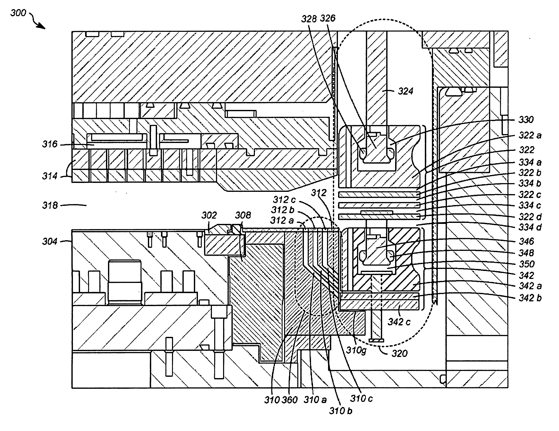
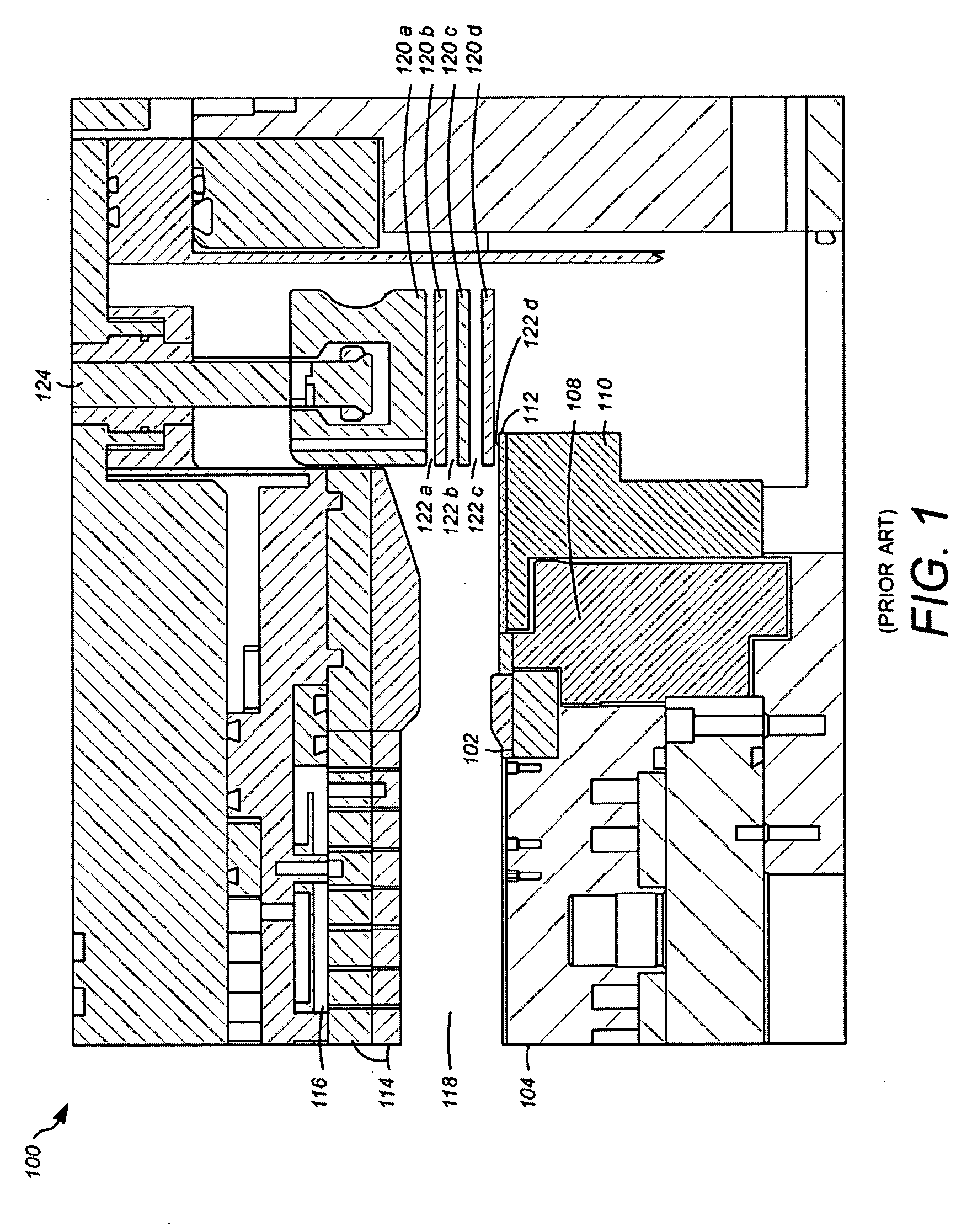
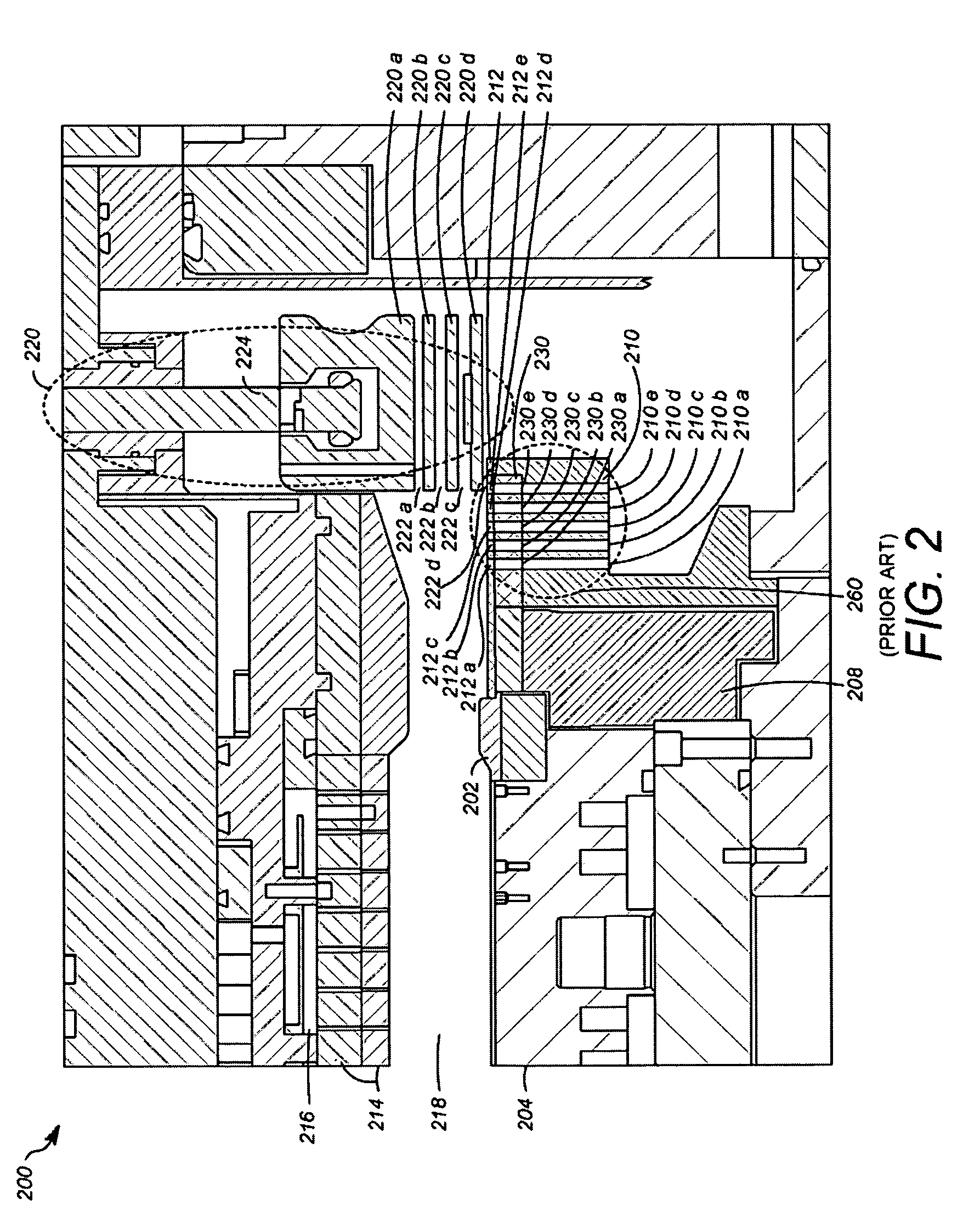
[0018]Due to the competitive advancement in the semiconductor industry, a significant number of leading-edge process applications in plasma processing may require processing steps with ultra short process gas residence times. Shorter residence times may require an increased gas conductance range which may be a trade-off with hardware features for confining plasma. To increase gas conductance in a ve...


PUM

PropertyMeasurementUnit
radio frequenciesaaaaaaaaaa

Abstract

An apparatus for controlling gas flow conductance in a plasma processing chamber being configured with an upper electrode disposed opposite a lower electrode adapted to support a substrate is provided. The apparatus includes a ground ring configured to include a first set of radial slots formed therein. The apparatus also includes a confinement ring arrangement which includes at least a first set of collapsible confinement rings and a second set of collapsible confinement rings which is configured to movably couple to the first set of collapsible confinement rings. The apparatus further includes a mechanism configured at least to collapse and to expand the first set of collapsible confinement rings and the second set of collapsible confinement rings to control gas flow conductance through the first set of radial slots between (a) an unobstructed gas flow, ON state, and (b) an obstructed gas flow, OFF state.

Description

BACKGROUND OF THE INVENTION[0001]Advances in plasma processing have facilitated growth in the semiconductor industry. The semiconductor industry is a highly competitive market. The ability for a chip manufacturing company to be able to process a substrate in different processing conditions may give the manufacturing company an edge over the competitor. Thus, manufacturing companies have dedicated time and resources to identify methods and / or arrangements for improving substrate processing.[0002]A typical processing system that may be employed to perform substrate processing may be a capacitively-coupled plasma (CCP) processing system. The plasma processing system may be built to enable processing in a number of process parameters each of them having a wide range. However, in recent years, the types of devices that may be processed have become more sophisticated and ma) require more process control. For example, devices being processed are becoming smaller with finer features and may...

Claims


Application Information

Patent Timeline
Patent Type & Authority Applications(United States)
IPC IPC(8): H01L21/306G05D7/03
CPCC23C16/45523C23C16/509G05D7/0635H01J37/32642H01J37/32449H01J37/32623H01J37/3244Y10T137/0324
Inventor FISCHER, ANDREAS
Owner LAM RES CORP
Why Eureka
Try Eureka