Method and apparatus for controlling Anti-blooming timing to reduce effects of dark current

a technology of anti-blooming timing and dark current, which is applied in the field of semiconductor imaging devices, can solve the problems of blooming, dark current, and corrupting the ability of pixel cells to correctly capture images, and achieve the effects of reducing the size of the pixel cell, and reducing the pixel cell siz

Active Publication Date: 2009-08-20
APTINA IMAGING CORP
View PDF29 Cites 4 Cited by
  • Summary
  • Abstract
  • Description
  • Claims
  • Application Information

AI Technical Summary

Problems solved by technology

One drawback to a typical pixel cell architecture is blooming.
Blooming is a deteriorating effect on the captured image that occurs when a photo-diode or photoactive region in a pixel cell is saturated and excess electric charge spills into adjacent photo-diodes or photoactive regions, thus corrupting their ability to correctly capture an image.
Another common problem in electronic imagers is dark current.
Dark current results in extraneous charge being collected by the pixel cells even when the imager is not exposed to light and, thus, erroneous pixel values being generated.

Method used


Image

  • Method and apparatus for controlling Anti-blooming timing to reduce effects of dark current
  • Method and apparatus for controlling Anti-blooming timing to reduce effects of dark current
  • Method and apparatus for controlling Anti-blooming timing to reduce effects of dark current

Examples


Embodiment Construction

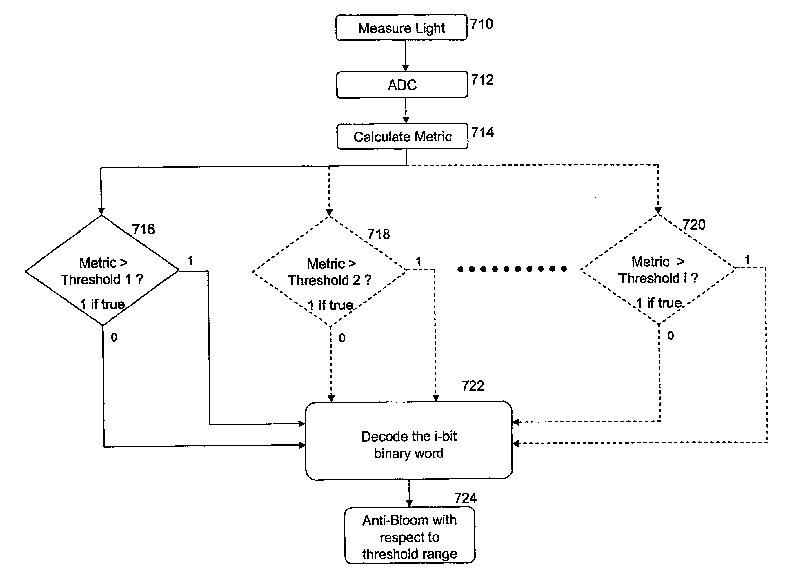
[0015]An electronic imager typically includes an array of pixel cells for capturing an image. Each pixel cell includes a photo-sensor for photocurrent generation during an integration time when the electronic imager is capturing an image. During the integration time, the photo-sensor accumulates electric charge in response to impinging photons.

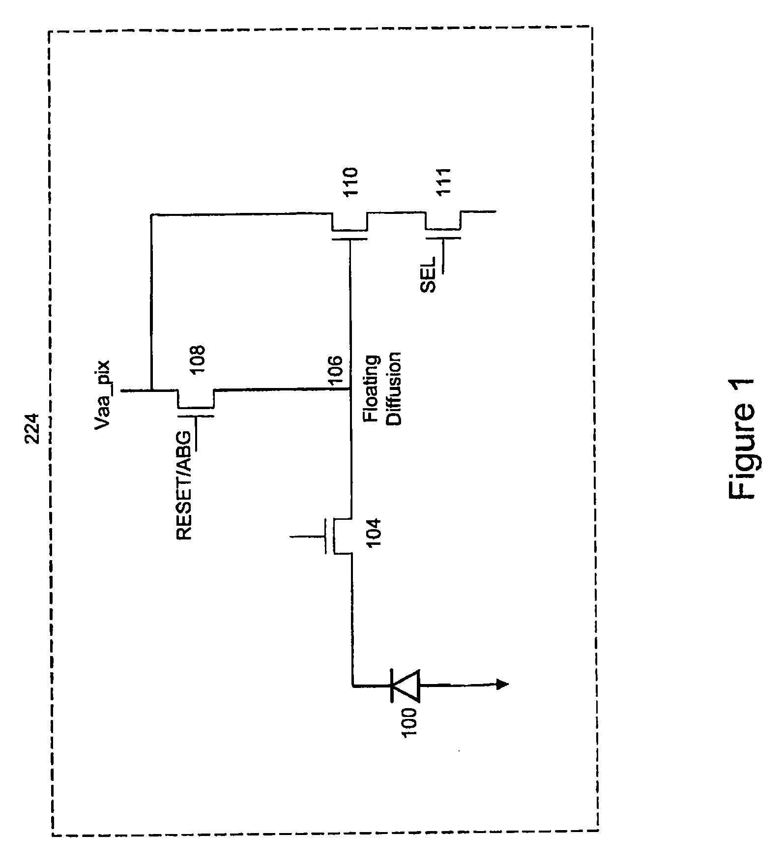
[0016]In one example, an electronic imager may consist of complimentary metal-oxide semiconductor (CMOS) active pixel sensor (APS) pixel cells. As described above, CMOS pixel cells typically consists of a photo-diode for photocurrent generation to generate an accumulated charge and a floating diffusion to store the charge accumulated by the photodiode. Although photo charges are generated as electron-hole pairs, it is the accumulation of the photoelectrons in the reverse-biased photodiode that produces the pixel values addressed here. In addition, a CMOS APS pixel may include a reset transistor for resetting accumulated charge produced by the ...


PUM


Abstract

An electronic imager includes a plurality of pixels having photosensors for accumulating charge corresponding to individual pixel values of a sensed image. Each of the pixels includes an anti-blooming function which allows charge in excess of a predetermined amount to be drained from the photosensor thus reducing the charge from the pixel that migrates to adjacent pixels. The imager also includes circuitry which controls the anti-blooming function in response to image intensity to reduce dark current in the imager caused by the anti-blooming function.

Description

CROSS REFERENCE TO RELATED APPLICATIONS[0001]This application is a Continuation of U.S. application Ser. No. 11 / 942,771, filed Nov. 20, 2007, the contents of which are incorporated herein by reference.BACKGROUND OF THE INVENTION[0002]The present invention concerns semiconductor imaging devices and, in particular, such devices having anti-blooming features.[0003]A semiconductor imaging device typically includes an array of pixel cells for capturing an image. Each pixel cell includes a photo-sensor which collects photoelectrons generated during an exposure time when the electronic imager is capturing an image. During the exposure time, the photo-sensor accumulates electric charge, (i.e. electron-hole pairs) in response to impinging photons.[0004]In one example, an electronic imager may include an array of complimentary metal-oxide semiconductor (CMOS) active pixel sensor (APS) pixel cells. CMOS pixel cells typically consist of a photo-diode for photocurrent generation, a reset transis...

Claims


Application Information

Patent Timeline
Patent Type & Authority Applications(United States)
IPC IPC(8): H04N5/217H04N5/335H04N5/228H04N5/359H04N5/361H04N5/374
CPCH01L27/14656H04N5/3591H04N5/374H04N5/361H04N5/3592H04N25/621H04N25/622H04N25/63H04N25/76
Inventor JOHNSON, RICHARD SCOTT
Owner APTINA IMAGING CORP
Why Eureka
Try Eureka