Light emitting device with translucent ceramic plate

a technology of translucent ceramics and light emitting devices, which is applied in solid-state devices, discharge tubes/lamp details, light sources, etc., can solve the problems of reduced radiation transparency, strong light scattering, and reduced luminosity of ceramic members, so as to improve the luminance intensity of light emitting devices.

Active Publication Date: 2009-08-27
SCHOTT AG
View PDF26 Cites 72 Cited by
  • Summary
  • Abstract
  • Description
  • Claims
  • Application Information

AI Technical Summary

Benefits of technology

[0013]Another embodiment provides a method for improving the luminance intensity of a light emitting device comprising providing a light emitting component, positioning at least one sintered ceramic plate comprising a multiphasic material over the light emitting component, said multiphasic material compri

Problems solved by technology

However, since the particle size of YAG phosphor powder utilized for this system is around 1-10 μm, the YAG powders dispersed in the encapsulant resin medium can cause strong light scattering.
However, these ceramic members can also suffer from decreased luminosity due to air voids formed during the formation of the ceramic.
These air voids can result in reduced transparency to radiation emitted by the LED and/or increased levels of backscattering.
Since the refractive index of the air as compared to the ceramic material is relatively large (on the order of 0.5 to 1.0), minute amounts of these air pockets can cause disproportionately large amount of backscattering.
However increased levels of non-emissive materials can still result in increased levels of scattering centers, and reducing the overall luminosity of the ceramic plate.
This high differential results in an increased c

Method used


Image

  • Light emitting device with translucent ceramic plate
  • Light emitting device with translucent ceramic plate
  • Light emitting device with translucent ceramic plate

Examples


example 1

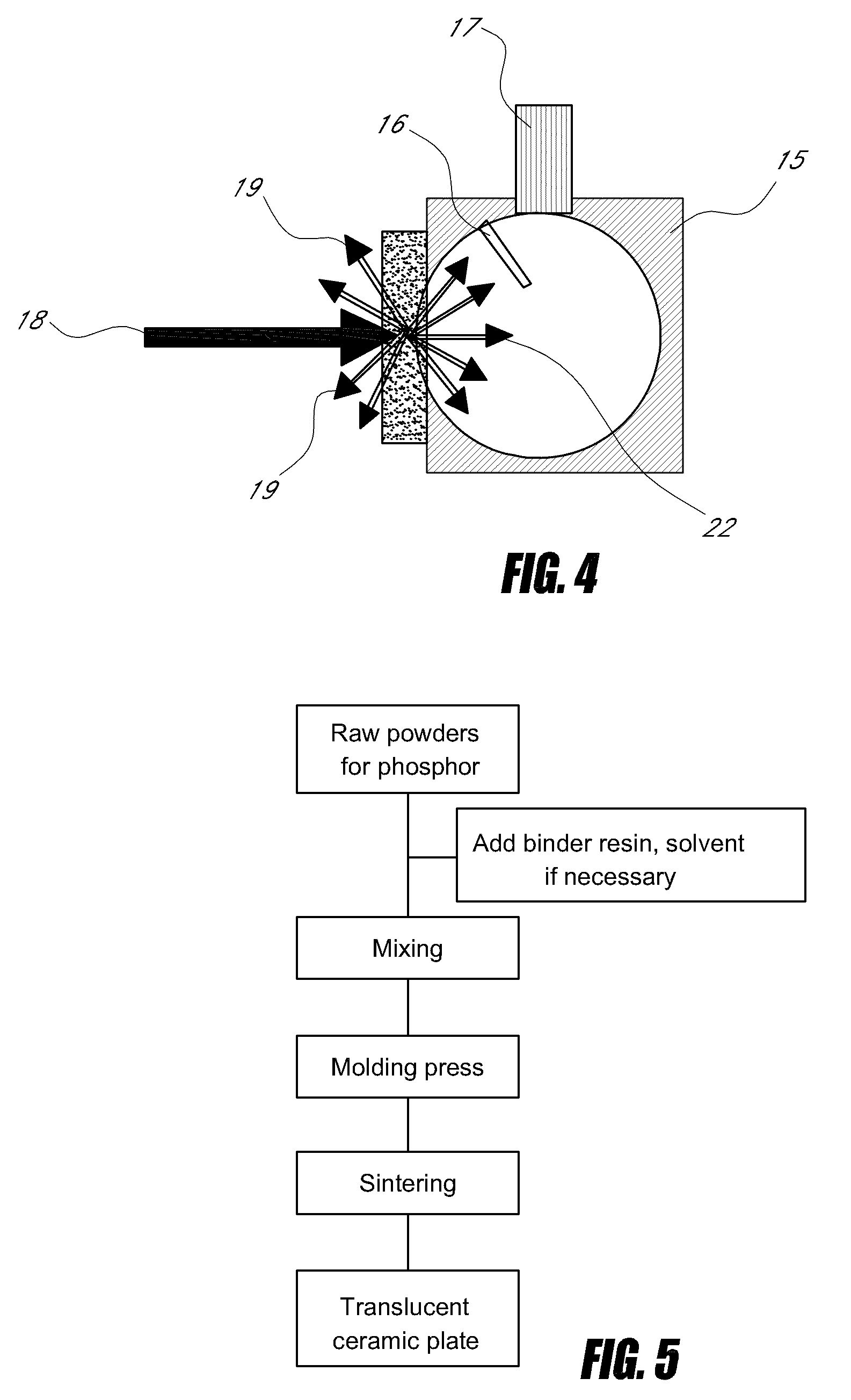
Preparation of Raw Particles by Using Inductively Coupled RF Thermal Plasma Pyrolysis

[0063]0.14923 mol (14.29 g) of Yttrium (III) nitrate hexahydrate (99.9% pure, Sigma-Aldrich), 0.25 mol (23.45 g) of Aluminum nitrate nonahydrate (99.97% pure, Sigma-Aldrich), and 0.015 mol (0.081 g) of Cerium (III) nitrate hexahydrate (99.99% pure, Sigma-Aldrich) were dissolved in 250 ml of deionized water, followed by ultrasonication for 30 min to prepare the transparent precursor solution. This precursor solution of 0.4 M was carried into a plasma reaction chamber via an atomization probe using a liquid pump.

[0064]All deposition experiments were conducted with an RF induction plasma torch (TEKNA Plasma System, Inc PL-35) operating at 3.3 MHz. For the deposition experiments, the chamber pressure was kept at around 25 kPa-35 kPa, and the RF generator plate power was in the range of 10-12 kW. Both the plate power and the deposition pressure are user-controlled parameters. Argon was introduced into th...

example 2

[0070]Sintered ceramic plate samples were made using annealed nano-powders instead of as-synthesized nano-powders from RF plasma. The nano-powder prepared by previously mentioned RF plasma method was annealed at 1200° C. for 2 hrs in a H2 / N2=3% / 97% ambient using a quartz tube furnace (MTI Corporation GSL-1600×) at 1 atm. The rate of increase of temperature was 10° C. / min. After the annealing, yellowish colored powder was obtained and yttrium aluminum garnet crystalline phase was determined by XRD. The average diameter after annealing obtained from BET measurement was 129 nm.

[0071]The same procedures for preparing the sintered ceramic plates described in Example 1 were followed. The loading quantities of dry powders spread out into die set with 3 mm of diameter were 45.0, 47.5, 50.0, 52.5, 55.0, and 57.5 mg. The crystalline phase of all ceramic plate samples was determined as yttrium aluminum garnet by XRD. The thicknesses of ceramics plates were summarized in Table 2.

[0072]In the sa...

example 3

[0080]Multiphasic sintered ceramic plate: sample 3-1 was made using the RF plasma method described in Example 1. The precursor solution was prepared by dissolving 0.14923 mol (14.29 g) of Yttrium (III) nitrate hexahydrate (99.9% pure, Sigma-Aldrich), 0.25625 mol (24.03 g) of Aluminum nitrate nonahydrate (99.97% pure, Sigma-Aldrich), and 0.015 mol (0.081 g) of Cerium (III) nitrate hexahydrate (99.99% pure, Sigma-Aldrich) in 250 ml of deionized water, followed by ultrasonication for 30 min. The nano-powders prepared using this precursor solution have additional material Al2O3 for forming the second phase. The nano-powders were annealed at 1200° C. for 2 hrs in a H2 / N2=3% / 97% ambient. The rate of the increase of temperature was 5° C. / min. After the annealing, yellowish colored powder was obtained and yttrium aluminum garnet crystalline phase was determined by XRD. Small XRD peaks of Al2O3 phase were also detected in accordance with the amount of second phase material in the Al-rich com...


PUM

PropertyMeasurementUnit
Fractionaaaaaaaaaa
Fractionaaaaaaaaaa
Fractionaaaaaaaaaa

Abstract

A light emitting device comprising a light emitting component that emits light with a first peak wavelength, and at least one sintered ceramic plate over the light emitting component is described. The at least one sintered ceramic plate is capable of absorbing at least a portion of the light emitted from said light emitting component and emitting light of a second peak wavelength, and has a total light transmittance at the second peak wavelength of greater than about 40%. A method for improving the luminance intensity of a light emitting device comprising providing a light emitting component and positioning at least one translucent sintered ceramic plate described above over the light emitting component is also disclosed.

Description

CROSS-REFERENCE TO RELATED APPLICATIONS[0001]This application claims priority to U.S. Provisional Application Nos. 61 / 030,496, filed Feb. 21, 2008, and 61 / 153,227, filed Feb. 17, 2009, both of which are hereby incorporated by reference in their entireties.BACKGROUND[0002]1. Field of the Invention[0003]The present invention relates to a light emitting device comprising translucent ceramic plates.[0004]2. Description of the Related Art[0005]Solid state light emitting devices such as light emitting diode (LED), organic light emitting diode (OLED) or sometimes called organic electroluminescent device (OEL), and inorganic electroluminescent device (IEL) have been widely utilized for various application such as flat panel display, indicator for various instrument, signboard, and ornamental illumination, etc. As the emission efficiency of these light emitting devices continues to improve, applications that require much higher luminance intensity, such as automobile headlights and general l...

Claims


Application Information

Patent Timeline
IPC IPC(8): H01J1/62
CPCB82Y30/00H05B33/14C04B35/62675C04B35/6268C04B35/63416C04B35/6342C04B2235/3206C04B2235/3217C04B2235/3222C04B2235/3225C04B2235/3229C04B2235/3418C04B2235/3427C04B2235/5454C04B2235/656C04B2235/6581C04B2235/80C04B2235/9653C04B2235/9661C09K11/7774H01L25/0753H01L33/502C04B35/44H01L2924/0002H01L2924/00
Inventor NAKAMURA, TOSHITAKAFUJII, HIRONAKAMIYAGAWA, HIROAKIMUKHERJEE, RAJESHZHANG, BINMOCHIZUKI, AMANE
Owner SCHOTT AG
Why Eureka
Try Eureka