

Micro-optical image stabilizer
a micro-optical and image stabilizer technology, applied in the field of image stabilizers, can solve the problem that the size of the image stabilizer is also getting smaller
- Summary
- Abstract
- Description
- Claims
- Application Information
AI Technical Summary
Benefits of technology
Problems solved by technology
Method used
Image

Examples
first embodiment
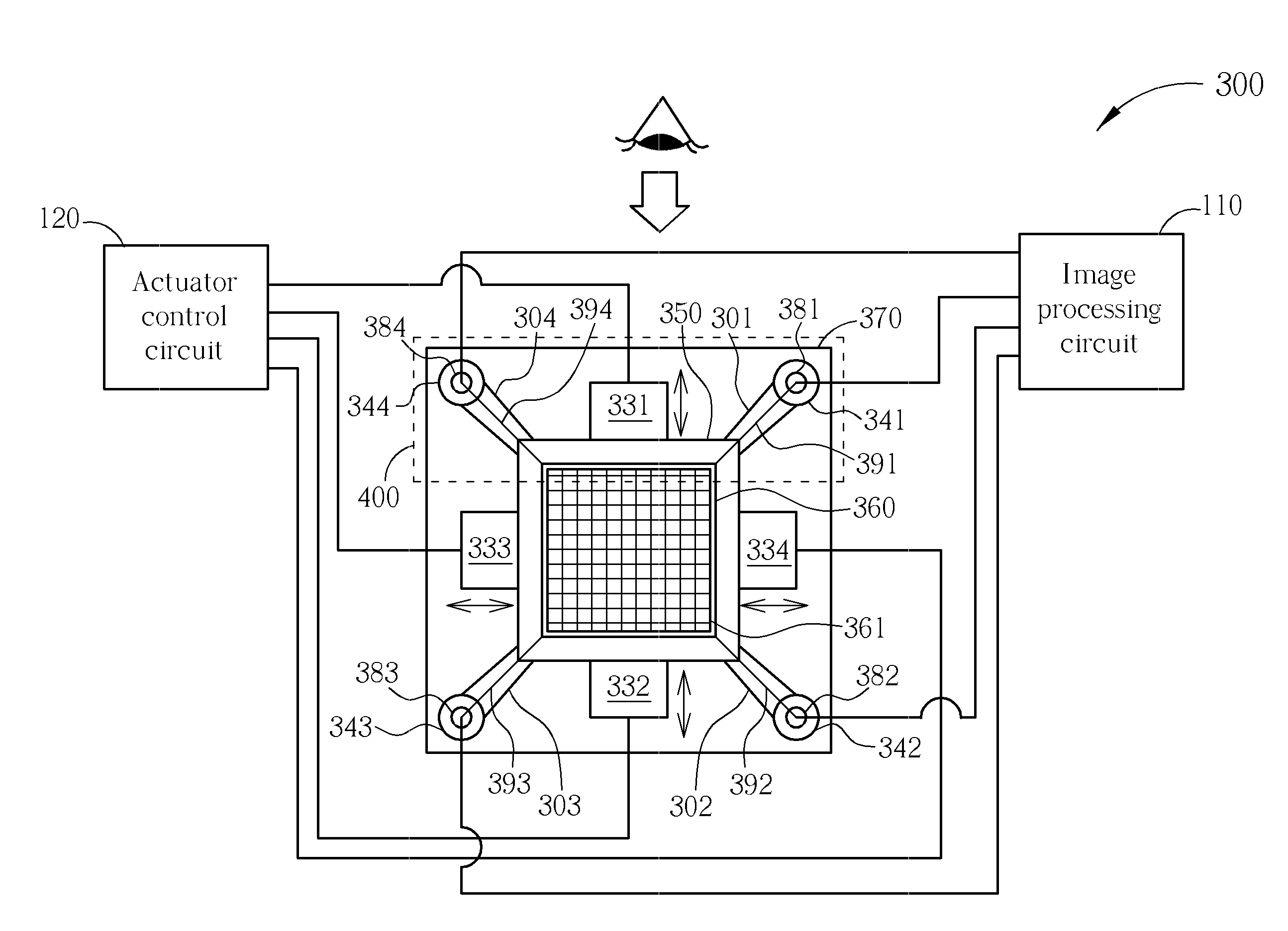
[0032]Please refer to FIG. 3. FIG. 3 is a diagram illustrating a first embodiment according to the micro-optical image stabilizer 300 of the present invention. As shown in FIG. 3, the image stabilizer 300 comprises an image processing circuit 110, an actuator control circuit 120, 4 sets of actuators 331-334, a substrate 370, a carrier 350, an image sensor 360, 4 anchors 341-344, 4 conducting pads 381-384, 4 conducting lines 391-394, 4 conducting pads 3811-3844 (not shown), and 4 flexible suspensions 301-304. The image sensor 360 comprises an image sensing area 361. The actuator control circuit 120 is coupled to the actuators 331-334 for controlling the movement of the actuators 331-334. One end of each of the actuators 331-334 is fixed on the substrate 370 and the other end of each of the actuators 331-334 is fixed on the carrier 350. In this way, the actuator control circuit 120 respectively controls the actuators 331-334 so as to move the position of the carrier 350 relative to th...
second embodiment
[0037]Please refer to FIG. 6. FIG. 6 is a diagram illustrating the cross-section of the image stabilizer 300 of the present invention fabricated by flip chip bonding. FIG. 6 is similar to FIG. 4 and the difference is: in FIG. 6, the image sensing area 361 is set between the image sensor 360 and the substrate 370. Consequently, the carrier 350 and the substrate 370 have to be accordingly disposed with holes to provide optical paths for the optical images. Thus, the optical images form on the image sensing area 361 through the substrate 370. Therefore, according to FIG. 4 and FIG. 6, users have two choices to design the image sensor 360 and the image sensing area 361, which further increases convenience.
[0038]Please refer to FIG. 14. FIG. 14 is a diagram illustrating the second embodiment of the image stabilizer 300 of the present invention fabricated by wire bonding. FIG. 14 is similar to FIG. 12 and the difference is: in FIG. 14, the image sensing area 361 is set between the image s...
third embodiment
[0046]Please refer to FIG. 17. FIG. 17 is a diagram illustrating a third embodiment according to the micro-optical image stabilizer 1700 of the present invention. FIG. 17 shows the top view of the image stabilizer 1700. As shown in FIG. 17, the image stabilizer 1700 comprises an image processing circuit 110, an actuator control circuit 120, a substrate 370, an image sensor 360, 4 anchors 1711a-1741a, 4 anchors 1711b-1741b, 4 conducting pads 1712a-1742a, 4 conducting pads 1712b-1742b, 4 anchors 1715-1745, 4 conducting pads 1718-1748, 4 conducting lines 1717-1747, 4 conducting pads 1716-1746, 4 flexible suspensions 1714-1744, 4 connecting arms 1713-1743 (some parts of the connecting arms 1713-1743 are covered by the image sensor 360 and thus not shown in FIG. 17). The image sensor 360 comprises an image sensing area 361 and 4 conducting pads 461-464 coupled to the image sensing area 361 for transmitting image signals. The image stabilizer 1700 further comprises 4 actuators ACT1-ACT4 d...
PUM
 Abstract
Description
Claims
Application Information