Transient blocking unit using normally-off device to detect current trip threshold
a technology of current trip threshold and transient blocker, which is applied in the direction of emergency protective arrangements for limiting excess voltage/current, electrical apparatus responsive to excess voltage, etc., can solve the problem that the threshold voltage of a depletion mode transistor is a relatively poorly controlled device parameter
- Summary
- Abstract
- Description
- Claims
- Application Information
AI Technical Summary
Benefits of technology
Problems solved by technology
Method used
Image

Examples
embodiment 700
[0042]According to an alternate embodiment 700 of the current invention, shown in FIG. 7, the circuit overcomes the susceptibility to threshold variation by using a small low voltage enhancement mode transistor 702 as a voltage controlled switch to detect the threshold of the trip current. Here, the small transistors 702 are low voltage enhancement mode devices. The Rdson of these devices is chosen appropriately so they will not slow the turn on of the high voltage NMOS. The threshold of these devices in this example is set at about 1V.
[0043]In this case, and for simplicity, the gate drive resistors 704 are connected to the source 114 of the NMOS device 102, but as mentioned previously could, under certain design conditions, be connected to the drain instead (see FIG. 8 for example), for possible advantage in Rdson and linearity.
[0044]Devices 702 are the same depletion NMOS, and the PJFET 108 is also the same as the exemplary design previously discussed.
[0045]Simulating the performa...
embodiment 1400
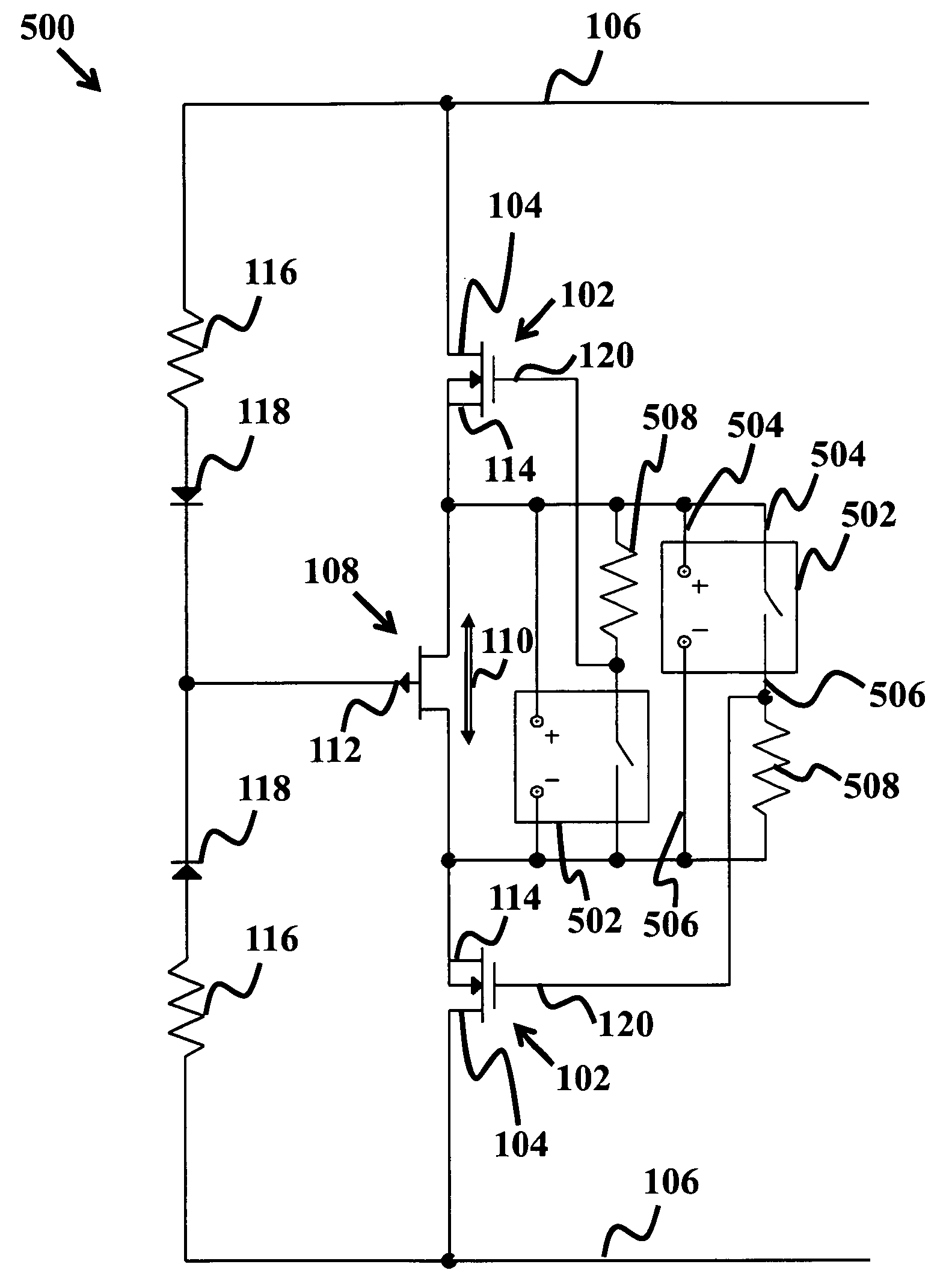
[0051]The present invention has now been described in accordance with several exemplary embodiments, which are intended to be illustrative in all aspects, rather than restrictive. Thus, the present invention is capable of many variations in detailed implementation, which may be derived from the description contained herein by a person of ordinary skill in the art. For example, FIG. 14 shows the a further embodiment 1400 having sensing terminals 504 of the switch 502 connected between the source 114 of the NMOS 102 and the output terminals 106. This has the advantage of allowing the resistance of the reversed NMOS 102 to be added to the PJFET 108 resistance, so giving a higher sensing voltage for a given current, making it easier to use with an enhancement mode transistor. This is particularly advantageous for low current threshold TBU's.
[0052]It is understood that other arrangements with the diodes and / or resistors are possible in connecting the transistors, switches and terminals, ...
PUM
 Abstract
Description
Claims
Application Information